Die bonding method and terminal
A die-bonding and terminal technology, applied in electrical components, circuits, semiconductor devices, etc., can solve the problems of slow die-bonding speed, low alignment accuracy, affecting the use of MiniLED, etc., and achieve high die-bonding efficiency and improve die-bonding accuracy. Effect
- Summary
- Abstract
- Description
- Claims
- Application Information
AI Technical Summary
Problems solved by technology
Method used
Image
Examples
Embodiment 1
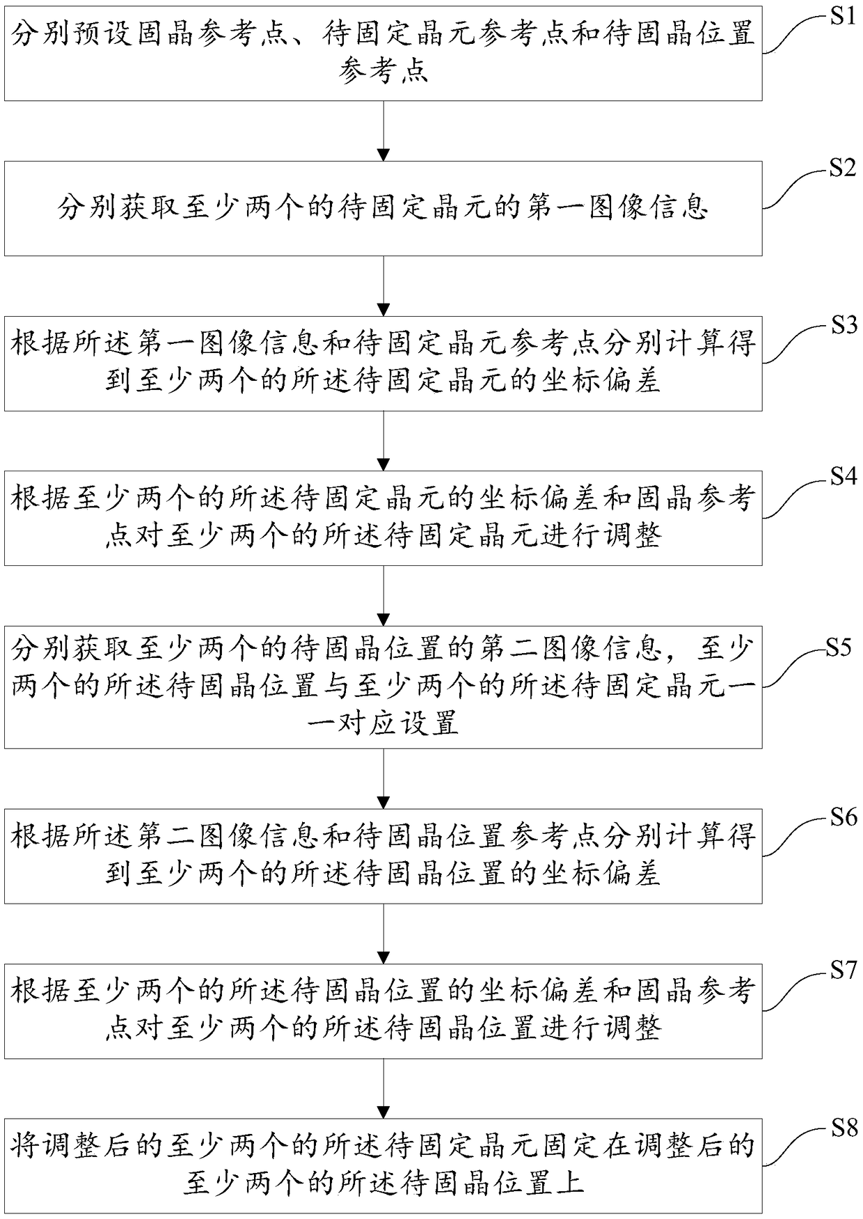
[0075] Please refer to figure 1 , Embodiment 1 of the present invention is:
[0076] A kind of solid crystal method, comprises the steps:
[0077] S1. Respectively preset the reference point for die bonding, the reference point for the wafer to be fixed, and the reference point for the position of the die to be bonded. The settings of the three reference points are all carried out in the same coordinate system. The reference point for die bonding is the specific coordinates at which the wafer to be fixed is fixed at the position to be bonded. Here, it specifically refers to the coordinates in the X and Y directions on the horizontal plane. Both the reference point of the wafer to be fixed and the reference point of the position of the wafer to be fixed refer to the coordinates in the X and Y directions on the horizontal plane.
[0078] S2. Respectively acquire first image information of at least two wafers to be fixed. The first image information is obtained through a large...
Embodiment 2
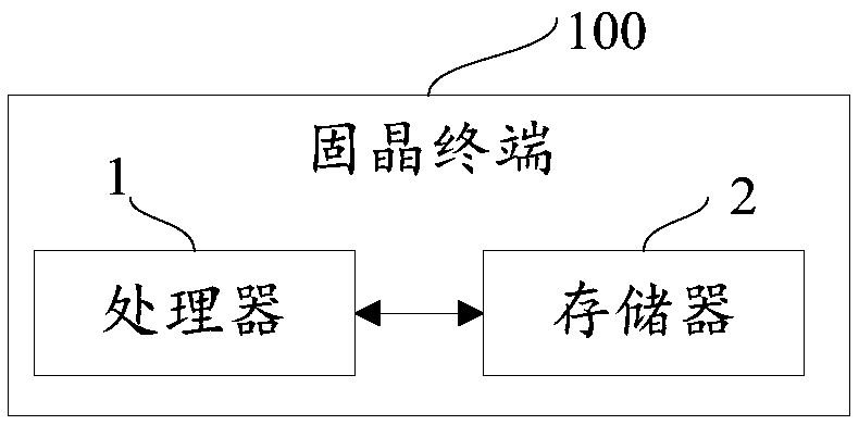
[0086] Please refer to figure 2 , the second embodiment of the present invention is:
[0087] A die-bonding terminal 100, corresponding to the method in Embodiment 1. The die-bonding terminal 100 includes a processor 1, a memory 2, and a computer program stored in the memory 2 and operable on the processor 1,
[0088] When the processor 1 executes the computer program, the following steps are implemented:
[0089] Respectively preset the reference point of die bonding, the reference point of wafer to be fixed and the reference point of the position of die to be bonded;
[0090] respectively acquiring first image information of at least two wafers to be fixed;
[0091] Calculate and obtain at least two coordinate deviations of the wafer to be fixed according to the first image information and the reference point of the wafer to be fixed;
[0092] adjusting at least two of the wafers to be fixed according to the coordinate deviation of the at least two wafers to be fixed an...
PUM
 Abstract
Description
Claims
Application Information

