A method for encapsulating LED modules used in automobile headlights
A technology for LED modules and automotive headlights, applied in semiconductor devices, electrical components, circuits, etc., can solve the problem of one-time use of lights, difficult design of peripheral heat dissipation, reduced chip reliability and service life, and reduced chip temperature. Chip reliability problems, such as optimizing the die-bonding operation process, improving the utilization rate of light, and reducing the moisture transmission rate.
- Summary
- Abstract
- Description
- Claims
- Application Information
AI Technical Summary
Problems solved by technology
Method used
Image
Examples
Embodiment 1
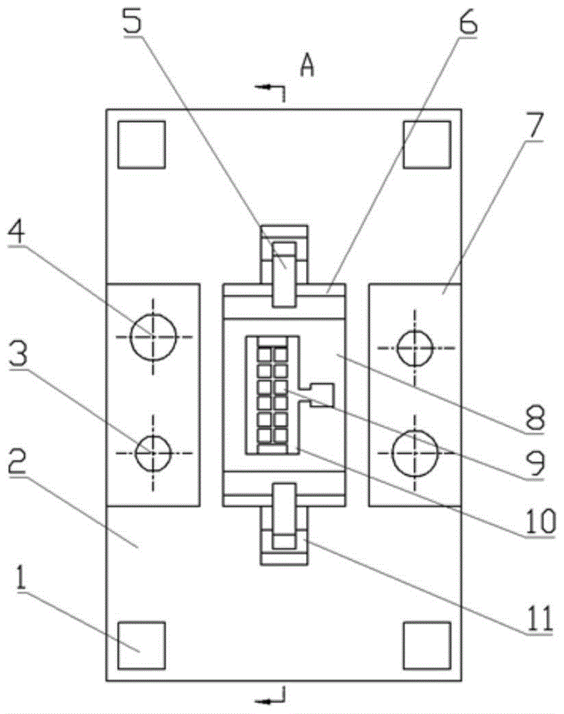
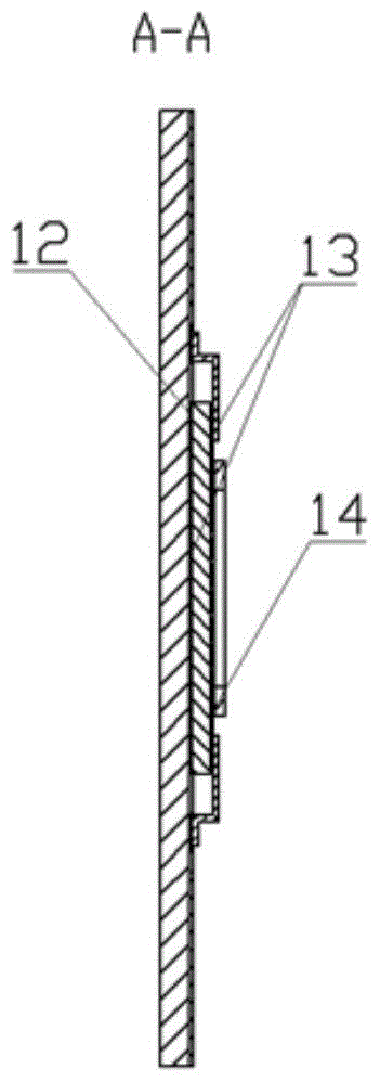
[0053] Referring to FIG. 4 , the AgSn solder 19 is drip-coated on the chip pad 9 with an amount of 0.04 μl. Stick the chip 18 on the pad 9 within a 45° deviation angle according to the electrode polarity, slightly adjust the chip with plastic tweezers to make the chip and the pad stick as much as possible, and place the module in a reflow oven for reflow curing. During the reflow process, the solder is liquid, and the surface tension is used to rotate the chip to coincide with the surface of the pad, and the die-bonding process is completed after cooling. Then drop-coat 0.05ml of AgSn solder on the upper surface of the lower substrate to make it as uniform as possible. Lay the middle substrate on the next substrate and manually adjust the relative position of the substrate. Since the non-contact surface is coated with solder resist white oil, the coating accuracy is determined by the position coordinates of the substrate, so the solder can be constrained in the bonding surface...
Embodiment 2
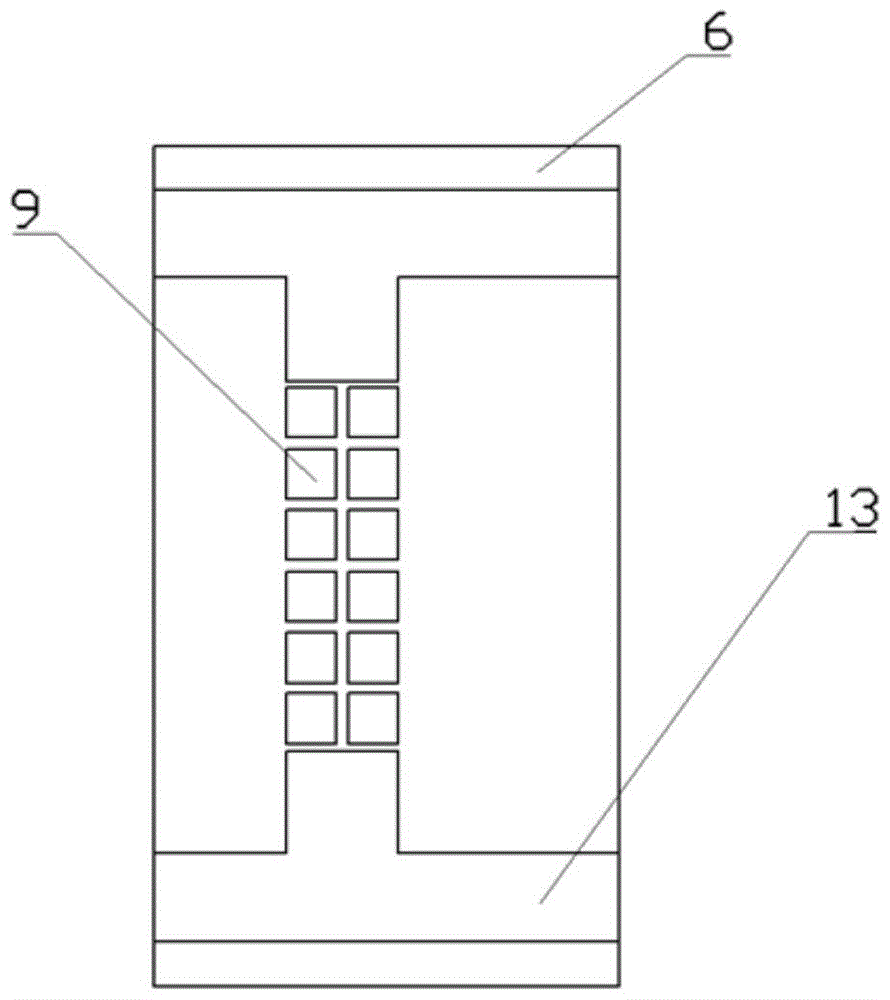
[0055] Referring to Figures 5-7, for the vertical chip packaging module, the substrate structure is as follows: the material and structure of the upper and lower substrates are basically the same as those in Embodiment 1, and the chip pad 9 of the middle substrate has the function of self-aligning the chip and conducting heat , also has the effect of conducting electricity, so the last pad needs to be directly connected to the peripheral circuit, and the solder is replaced with AuSn solder to reduce the resistance. Solder was dripped onto the die pad 9 in an amount of 0.04 μl. Put the chip 18 on the pad 9 within a 45° deviation angle according to the direction specified by the electrode polarity, with the positive electrode of the chip facing up and the negative electrode connected to the pad through solder. Put the module into the reflow oven for reflow curing. During the reflow process, the solder is liquid, and the surface tension is used to rotate the chip to coincide wit...
PUM
 Abstract
Description
Claims
Application Information


