Linear array image sensor image array and object surface defect detection method
A technology of sensor pixels and pixel arrays, which is applied in the direction of optical testing flaws/defects, instruments, measuring devices, etc., and can solve problems such as surface irregularities of target objects, differences in pixel response, and insufficient
- Summary
- Abstract
- Description
- Claims
- Application Information
AI Technical Summary
Problems solved by technology
Method used
Image

Examples
Embodiment 1
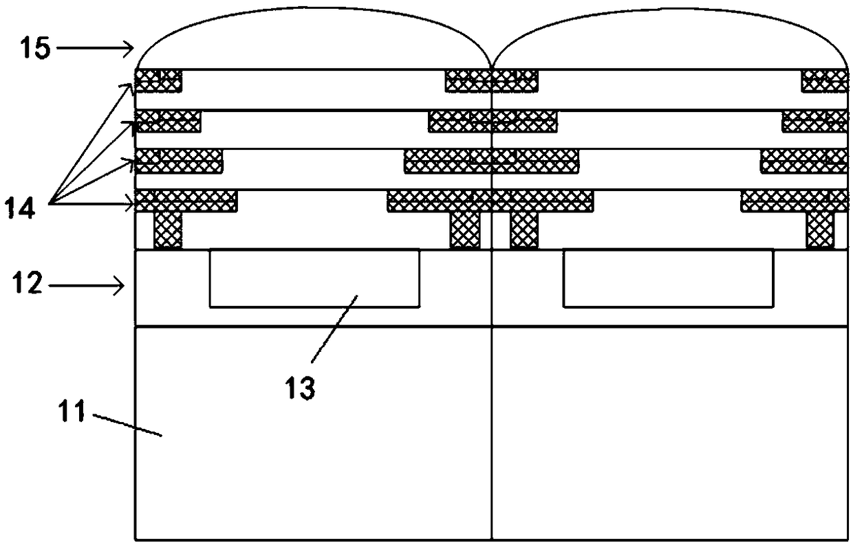
[0062] The pixel array of the line array image sensor of the present invention arranges three pixel array units, the number of pixel rows contained in the three pixel array units may be equal or not equal, and the number of pixel rows of the three pixel array units is all in the range of 1 to 10 between. The first pixel array unit is composed of A1-type pixels, the second pixel array unit is composed of B-type pixels, and the third pixel array unit is composed of A2-type pixels; A1-type pixels are A-type pixels with microlenses shifted to the left ; A2-type pixels are A-type pixels whose microlenses are shifted to the right.
[0063] Such as Figure 4 As shown, in this embodiment, each pixel array unit is selected to include a row of pixels; the pixel size is 5um x 5um, and the microlens apex height is 2um; the middle row is a B-type pixel, and its microlens 102 does not shift (the microlens coincides with the geometric center of the pixel) , the first row is an A1 type pixe...
Embodiment 2
[0084] The pixel array of the line array image sensor of the present invention arranges two pixel array units, the number of pixel rows contained in the two pixel array units may be equal or not equal, and the number of pixel rows of the two pixel array units are all in the range of 1 to 10 between. One pixel array unit is composed of type B pixels, and the other pixel array unit is composed of type A pixels.
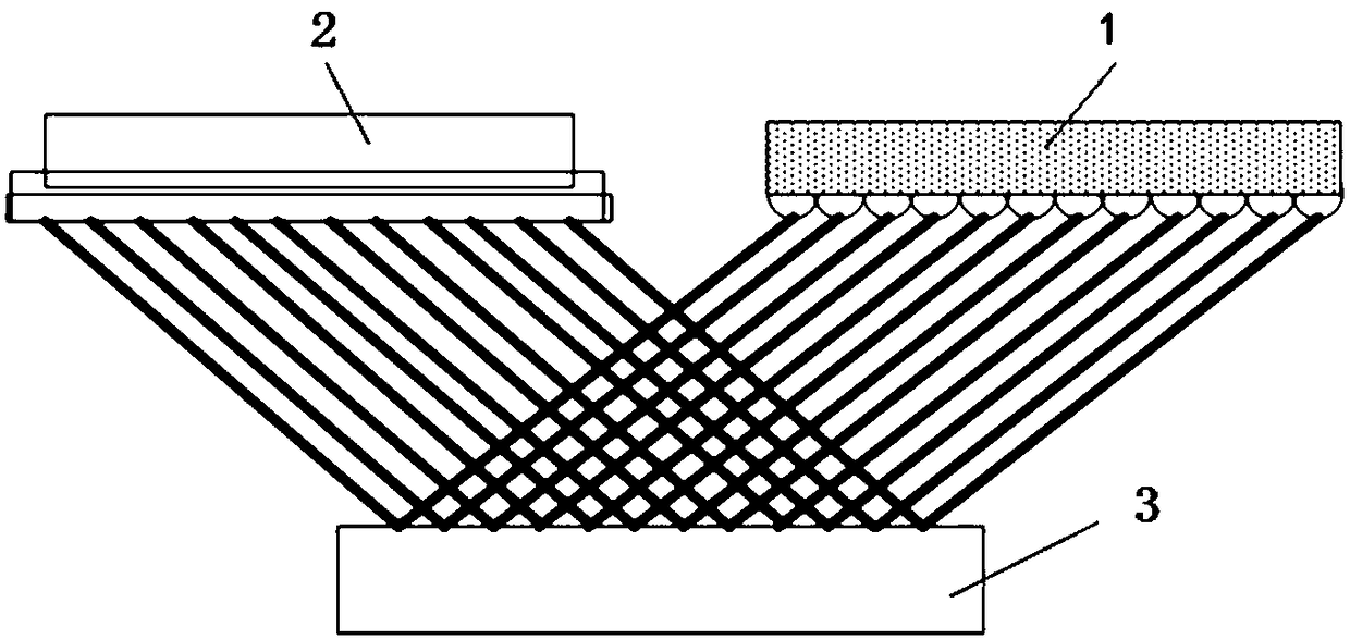
[0085] In this embodiment, each pixel array unit is selected to include a row of pixels; the pixel size is 5um x 5um, and the microlens apex height is 2um; the first row is a B-type pixel, and its microlens does not shift (the microlens coincides with the geometric center of the pixel); The second row is an A2-type pixel, and its microlens is offset by +1um (that is, the right offset is 1um).
[0086] This embodiment adopts the following method to obtain the angle response characteristic curve:
[0087] (1) Using the parallel light ray array image sensor pixel array, ...
PUM
| Property | Measurement | Unit |
|---|---|---|
| angle of incidence | aaaaa | aaaaa |
Abstract
Description
Claims
Application Information
 - R&D
- Intellectual Property
- Life Sciences
- Materials
- Tech Scout
- Unparalleled Data Quality
- Higher Quality Content
- 60% Fewer Hallucinations
Browse by: Latest US Patents, China's latest patents, Technical Efficacy Thesaurus, Application Domain, Technology Topic, Popular Technical Reports.
© 2025 PatSnap. All rights reserved.Legal|Privacy policy|Modern Slavery Act Transparency Statement|Sitemap|About US| Contact US: help@patsnap.com