Display substrate making method, display substrate and display device

A manufacturing method and display substrate technology, applied in semiconductor/solid-state device manufacturing, input/output process of data processing, optics, etc., to achieve the effect of improving image quality and texture

Inactive Publication Date: 2019-03-01
BOE TECH GRP CO LTD +1
View PDF6 Cites 0 Cited by
  • Summary
  • Abstract
  • Description
  • Claims
  • Application Information

AI Technical Summary

Problems solved by technology

[0003] In order to solve the above technical problems, an embodiment of the present invention provides a method for manufacturing a display substrate, a display substrate, and a display device, so as to solve the display problems of color moiré (Mura) and black spots or bright spots in the existing display substrates.

Method used


Image

  • Display substrate making method, display substrate and display device
  • Display substrate making method, display substrate and display device
  • Display substrate making method, display substrate and display device

Examples


Embodiment Construction

[0041] In order to make the technical problems, technical solutions and advantages to be solved by the present invention clearer, the following will describe in detail with reference to the drawings and specific embodiments.

[0042] The terms "first", "second" and the like in the description and claims of the present invention are used to distinguish similar objects, and are not necessarily used to describe a specific order or sequence. It is to be understood that the data so used are interchangeable under appropriate circumstances such that the embodiments of the invention described herein are, for example, capable of practice in sequences other than those illustrated or described herein.

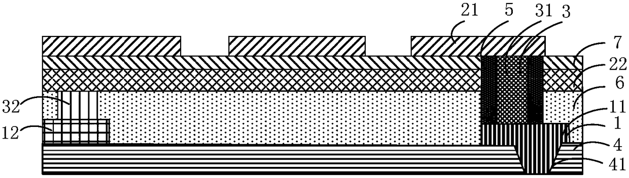
[0043] At present, a conventional TFT-LCD (Thin Film Transistor-Liquid Crystal Display) display substrate is composed of a first substrate and a second substrate, between which liquid crystals are filled, and spacers support to keep the liquid crystal cell thick and stable. Since the spa...


PUM

PropertyMeasurementUnit
thicknessaaaaaaaaaa

Abstract

The embodiment of the invention provides a display substrate making method, a display substrate and a display device. The display substrate making method comprises the steps that after a first conductive pattern is formed, a conductive column is formed on the first conductive pattern, and orthographic projection of the conductive column on a substrate body of the display substrate at least partially overlaps orthographic projection of a second conductive pattern on the substrate body. In this way, hole design is not needed on the display substrate, the first conductive pattern and the second conductive pattern located on different layers can be connected through the conductive column, the display problems that due to the fact that a spacer falls into a hole or PI liquid filling is insufficient, color moire fringes or dark spots or bright spots of the display substrate are caused are avoided, and the picture quality of display electronic products can be improved.

Description

technical field [0001] The invention relates to the field of display technology, in particular to a method for manufacturing a display substrate, a display substrate and a display device. Background technique [0002] With the continuous improvement of living standards and the continuous development of display technology, users have higher requirements for the image quality of display electronic products, making the display effect experience with finer image quality and more beautiful colors become the goal that the display field is constantly pursuing. However, the existing display substrates have display problems such as color moiré (mura), cross-color, black spots or bright spots. The above display problems are stumbling blocks that affect the improvement of display experience. Contents of the invention [0003] In order to solve the above technical problems, embodiments of the present invention provide a method for manufacturing a display substrate, a display substrate...

Claims


Application Information

Patent Timeline
Patent Type & Authority Applications(China)
IPC IPC(8): G02F1/1362G02F1/1343G02F1/1333G06F3/041H01L27/12H01L21/77
CPCG02F1/13338G02F1/134309G02F1/136227G06F3/0412G02F1/136295H01L27/124H01L27/1259
Inventor 张东东王志强
Owner BOE TECH GRP CO LTD
Why Eureka
Try Eureka