Display device, array substrate and manufacturing method thereof

A technology for array substrates and connection layers, which is applied in semiconductor/solid-state device manufacturing, semiconductor devices, electrical components, etc., and can solve problems such as poor display

Active Publication Date: 2020-02-21
BOE TECH GRP CO LTD +1
View PDF3 Cites 0 Cited by
  • Summary
  • Abstract
  • Description
  • Claims
  • Application Information

AI Technical Summary

Problems solved by technology

[0005] Although the current array substrate preparation process is becoming more and more mature, there are still many problems such as poor display

Method used


Image

  • Display device, array substrate and manufacturing method thereof
  • Display device, array substrate and manufacturing method thereof
  • Display device, array substrate and manufacturing method thereof

Examples


Embodiment Construction

[0030] Embodiments of the present invention are described in detail below, examples of which are shown in the drawings, wherein the same or similar reference numerals designate the same or similar elements or elements having the same or similar functions throughout. The embodiments described below by referring to the figures are exemplary only for explaining the present invention and should not be construed as limiting the present invention.

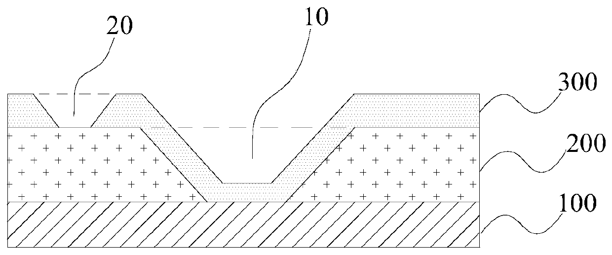
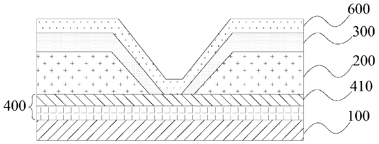
[0031] In one aspect of the present invention, the present invention provides an array substrate. According to an embodiment of the present invention, refer to figure 1 , the array substrate includes: a substrate 100 , a planarization layer 200 and a passivation layer 300 . According to an embodiment of the present invention, a planarization layer 200 is disposed on the substrate 100 . According to an embodiment of the present invention, the planarization layer 200 has a first via hole 10 . According to an embodiment of the present in...


PUM


Abstract

The invention discloses a display device, an array substrate and a preparation method of the array substrate. According to the embodiment of the invention, the array substrate comprises a substrate, aplanarization layer and a passivation layer, wherein the planarization layer is arranged on the substrate and is provided with a first via hole; and the passivation layer is arranged at one side, faraway from the substrate, of the planarization layer and is provided with a second via hole, wherein projections of the first via hole and the second via hole on the substrate are not overlapped. Therefore, a hole sleeving structure is not formed by the via hole of the polarization layer and the via hole of the passivation layer, the phenomenon of uneven display generated by the display device during displaying is relieved, the product yield is improved and the production cost is reduced.

Description

technical field [0001] The present invention relates to the field of display technology, in particular, to a display device, an array substrate and a preparation method thereof. Background technique [0002] Thin Film Transistor Liquid Crystal Display (TFT-LCD) is a type of liquid crystal display that uses thin film transistor technology to improve image quality, display quality and overall performance. TFT-LCD is favored by people for its large capacity, high definition and high-quality true color, and is widely used in TVs, flat-panel displays, projectors and electronic equipment. TFT-LCD uses an array substrate and a color film substrate to form a liquid crystal cell, and then undergoes subsequent processes such as polarizer coating, and finally forms a liquid crystal display device. Among them, the array substrate is one of the important components of the TFT-LCD. [0003] However, the current display devices, array substrates and manufacturing methods thereof still ne...

Claims


Application Information

Patent Timeline
Patent Type & Authority Patents(China)
IPC IPC(8): H01L27/12H01L21/77
Inventor 王文涛史大为杨璐徐海峰姚磊闫雷薛进进候林王金锋司晓文闫芳王培刘国梁
Owner BOE TECH GRP CO LTD
Why Eureka
Try Eureka