Touch screen manufacturing method and touch screen

A manufacturing method and touch screen technology, applied in instruments, computing, electrical digital data processing, etc., can solve problems such as various traces, uneven display brightness, abnormal appearance, etc., to avoid mura, improve appearance visibility, and increase efficiency. and performance effects

Active Publication Date: 2019-05-14
KUSN INFOVISION OPTOELECTRONICS
View PDF4 Cites 0 Cited by
  • Summary
  • Abstract
  • Description
  • Claims
  • Application Information

AI Technical Summary

Problems solved by technology

[0004] During the processing of the above-mentioned touch electrodes, it is necessary to cut the entire grid conductor layer, so as to pattern the grid conductor layer into the desired touch electrode shape. The conventional cutting method has obvious appearance at the dividing line. Visible cutting line, you can see the pattern of the grid electrode, when the product is composed, mura (the phenomenon of uneven brightness of the display, causing various traces) will appear, resulting in abnormal appearance, which is also a problem in the design of the grid electrode one

Method used


Image

  • Touch screen manufacturing method and touch screen
  • Touch screen manufacturing method and touch screen
  • Touch screen manufacturing method and touch screen

Examples


Embodiment Construction

[0037] The present invention is described below based on examples, but the present invention is not limited to these examples. In the following detailed description of the present invention, some specific details are described in detail. Those skilled in the art can fully understand the present invention without the description of these details. In order to avoid obscuring the essence of the present invention, well-known methods, processes, procedures, and components are not described in detail.

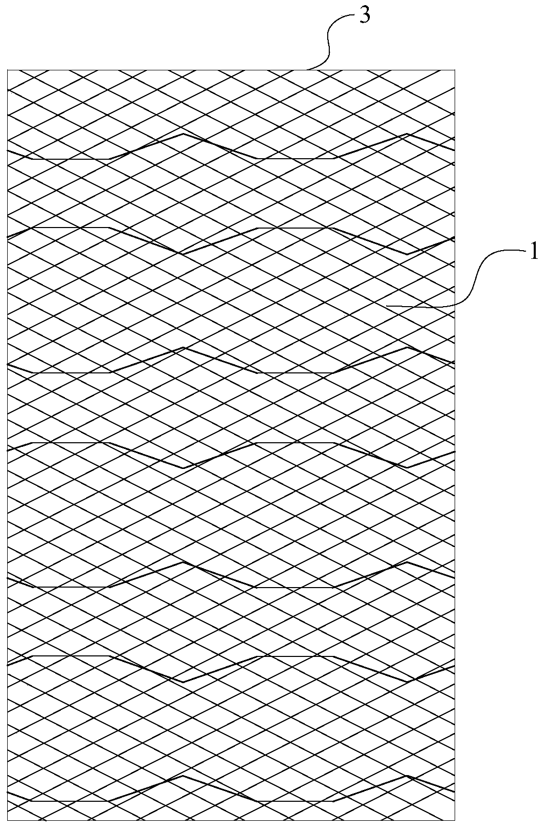
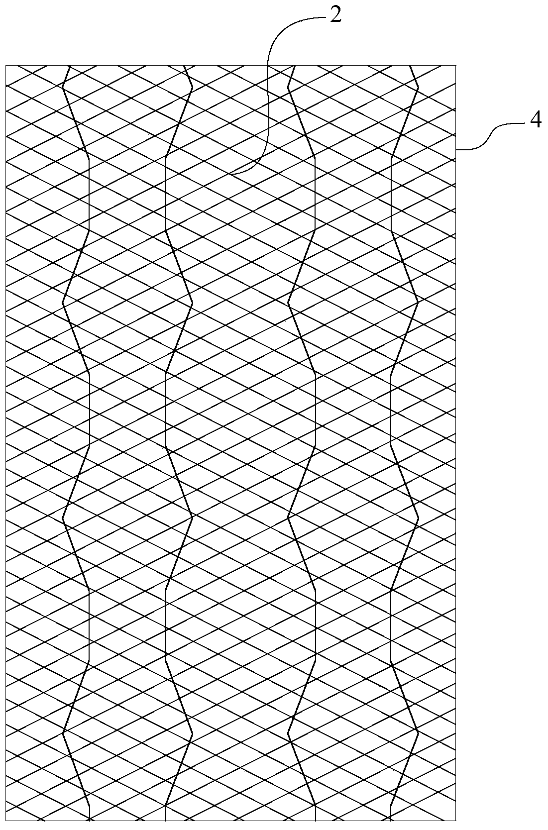
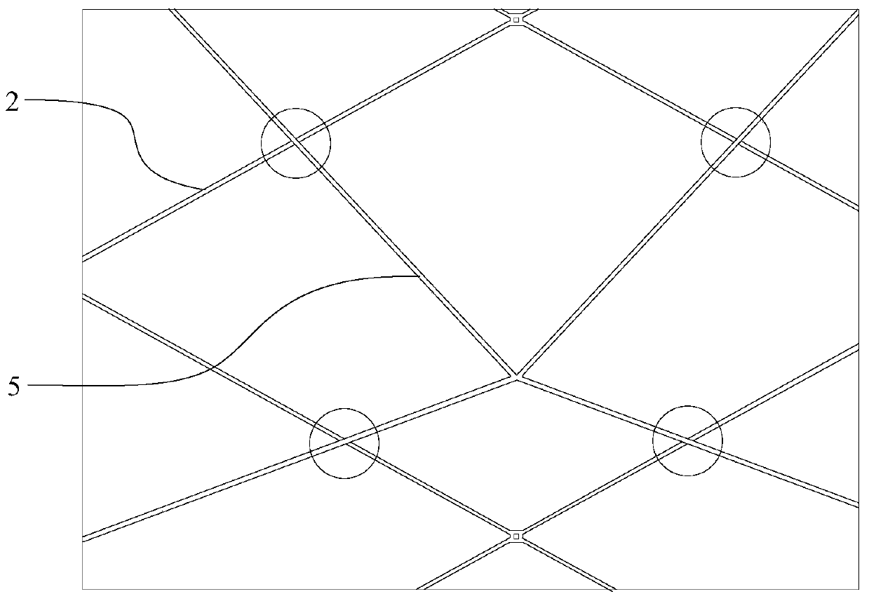
[0038] The present invention provides a method for manufacturing a touch screen. The touch screen includes a first grid electrode layer and a second grid electrode layer that are stacked, and the method includes:

[0039] Providing a laminated first grid conductor layer and a second grid conductor layer;

[0040] Cutting the first grid conductor layer to pattern the first grid conductor layer to form a first grid electrode;

[0041] Cutting the second grid conductor layer to pattern the se...


PUM


Abstract

The invention discloses a touch screen manufacture method and a touch screen. The touch screen manufacture method comprises the following steps: providing a first grid conductor layer and a second grid conductor layer, wherein the first grid conductor layer and the second grid conductor layer are overlaid; cutting the first grid conductor layer to carry out patterning on the first grid conductor layer to form a first electrode; cutting the second grid conductor layer to carry out patterning on the second grid conductor layer to form a second electrode; and moving at least one cutting point on the first grid conductor layer and / or second grid conductor layer to the grid line cross point of the first grid conductor layer and the second grid conductor layer adjacent to the cutting point. The color of the cut point and the color of an uncut point can be guaranteed to be a metal color, and the cut point and the uncut point do not have aberration so as to avoid a cutting line mura problem, improve the appearance visuality of the product and increase benefits and performance.

Description

Technical field [0001] The present invention relates to the field of touch technology, in particular to a touch screen manufacturing method and a touch screen. Background technique [0002] The touch electrodes used in existing touch screens are generally transparent conductive films, such as ITO (Indium Tin Oxides, indium tin oxide) thin films. Due to the high resistivity of ITO thin films, when the touch panel is enlarged, row electrodes or column electrodes are accompanied The increase in the resistance value between the terminals of, the detection sensitivity for changes in capacitance decreases, and it is difficult to make these electrodes operate as touch switches. [0003] In response to the above problems, a new touch screen structure is proposed in the prior art, which uses a grid-like conductor layer to form touch electrodes, so that the transmittance of the touch electrodes can reach more than 70%, and the resistance of the touch electrodes is reduced. . [0004] In the ...

Claims


Application Information

Patent Timeline
Patent Type & Authority Patents(China)
IPC IPC(8): G06F3/044
CPCG06F3/044G06F2203/04103
Inventor 邱峰青宋斌斌
Owner KUSN INFOVISION OPTOELECTRONICS
Why Eureka
Try Eureka