Grid driving circuit and driving method thereof

A gate drive circuit and level technology, applied to instruments, static indicators, etc., can solve problems such as abnormal display of display panels and large gradients

Active Publication Date: 2019-03-08
HEFEI BOE OPTOELECTRONICS TECH +1
View PDF10 Cites 0 Cited by
  • Summary
  • Abstract
  • Description
  • Claims
  • Application Information

AI Technical Summary

Problems solved by technology

[0003] The present invention provides a gate drive circuit and its drive method to solve the problem in the prior art that the gradient edge is relatively large, resulting in abnormal display of the display panel

Method used


Image

  • Grid driving circuit and driving method thereof
  • Grid driving circuit and driving method thereof
  • Grid driving circuit and driving method thereof

Examples


Embodiment 1

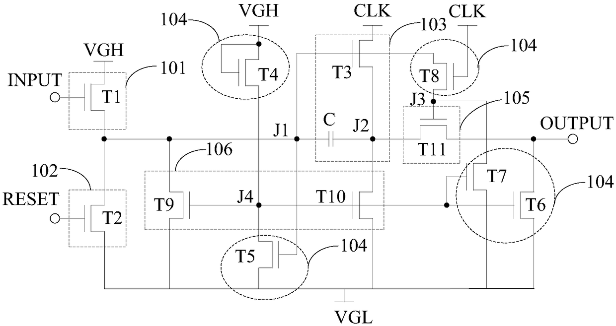
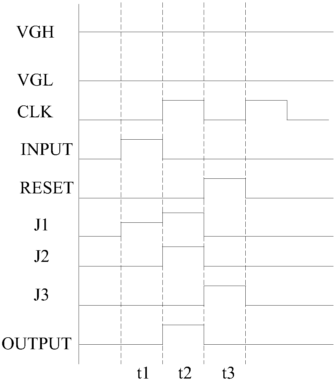
[0047] refer to figure 1 , shows a schematic structural diagram of a gate driving circuit provided by an embodiment of the present invention. The gate drive circuit 10 includes an input unit 101, a reset unit 102, a pre-output unit 103, an output control unit 104 and an output unit 105;

[0048] The input unit 101 is respectively connected to the input signal terminal INPUT and the first node J1, configured to receive an input signal, and set the potential of the first node J1 to a first level when the input signal is at a first level. level;

[0049] The reset unit 102 is respectively connected to the reset signal terminal RESET, the second level terminal and the first node J1, and is configured to receive a reset signal, and set the first node to J1 when the reset signal is at the first level. J1 is reset to the second level;

[0050] The pre-output unit 103 is respectively connected to the clock signal terminal CLK, the first node J1, and the second node J2, and is confi...

Embodiment 2

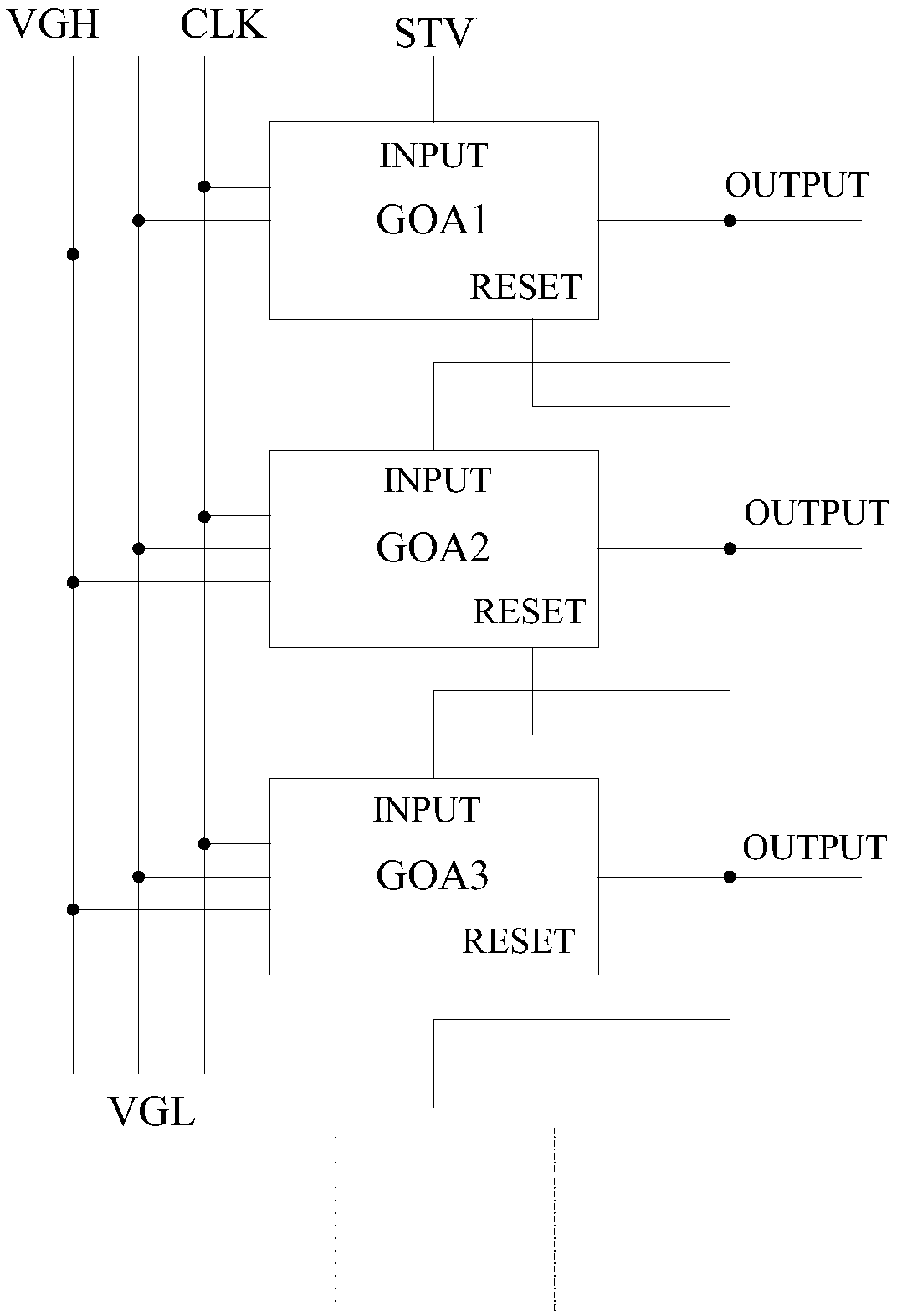
[0079] refer to image 3 , shows a schematic structural diagram of the gate driving cascade circuit provided by the embodiment of the present invention. The gate drive cascade circuit includes a plurality of gate drive circuits as described in Embodiment 1;

[0080] The input signal terminal INPUT of the first-stage gate drive circuit GOA1 is connected to the trigger signal terminal STV, and the output signal terminal OUTPUT is connected to the input signal terminal INPUT of the second-stage gate drive circuit GOA2;

[0081] Starting from the second-stage gate drive circuit GOA, the output signal terminal OUTPUT of each stage gate drive circuit is connected to the reset signal terminal RESET of the upper-stage gate drive circuit and the input signal of the next-stage gate drive circuit respectively. Terminal INPUT connection;

[0082] Each stage of the gate driving circuit is respectively connected to the first level terminal, the second level terminal and the clock signal t...

Embodiment 3

[0088] An embodiment of the present invention provides a display panel. The display panel includes the gate driving cascade circuit as described in the second embodiment.

[0089] In this embodiment, the gate drive cascade circuit includes multiple gate drive circuits as described in Embodiment 1; the input signal terminal INPUT of the primary gate drive circuit GOA1 is connected to the trigger signal terminal STV, and the output signal terminal OUTPUT is connected to the trigger signal terminal STV. The input signal terminal INPUT of the second-stage gate drive circuit GOA2 is connected; starting from the second-stage gate drive circuit GOA2, the output signal terminal OUTPUT of each stage gate drive circuit is respectively connected to the reset signal of the previous stage gate drive circuit Terminal RESET is connected to the input signal terminal INPUT of the gate drive circuit of the next stage; each gate drive circuit is connected to the first level terminal VGH, the sec...


PUM


Abstract

The invention provides a grid driving circuit and a driving method thereof. The grid driving circuit includes an input unit, a reset unit, a pre-output unit, an output control unit and an output unit.The input unit is respectively connected to an input signal terminal and a first node; the reset unit is respectively connected to a reset signal terminal, a second level terminal and the first node;the pre-output unit is respectively connected to a clock signal terminal, the first node and a second node; the output control unit is respectively connected to a first level terminal and the clock signal terminal, a third node, a fourth node and an output signal terminal; and the output unit is respectively connected to the second node, the third node and the output signal terminal. Through theembodiment of the invention, the gradual edge of an output signal of the grid driving circuit is reduced, and the abnormal display problem of a display panel can be avoided.

Description

technical field [0001] The present invention relates to the field of display technology, in particular to a gate drive circuit and a drive method thereof. Background technique [0002] In the product design process of the display panel, due to factors such as excessive load on the gate line and small drive transistors, the waveform of the output signal of the gate drive circuit is often not a perfect square wave, but has a gradient edge. When the gradient is small, that is, the gradient time is very short and the slope is very steep, there will be no obvious abnormality; but when the gradient is large, that is, the gradient time is long and the slope is gentle, it will take a certain time to fully open or close TFT (Thin Film Transistor, Thin Film Transistor) of the display panel. This situation will cause the display panel to display abnormally. Therefore, reducing the gradient edge is a technical problem to be solved urgently in the design of the gate drive circuit. Co...

Claims


Application Information

Patent Timeline
Patent Type & Authority Applications(China)
IPC IPC(8): G09G3/20
CPCG09G3/20
Inventor 余超智曲博文
Owner HEFEI BOE OPTOELECTRONICS TECH
Why Eureka
Try Eureka