A method and device for simulating biological optical synapse

A technology of organisms and devices, applied in the field of bionic synapses, can solve the problems of increasing power consumption and difficulty in obtaining electrical input signals directly, and achieve the effect of reducing power consumption

Active Publication Date: 2022-04-29
TSINGHUA UNIV
View PDF7 Cites 0 Cited by
  • Summary
  • Abstract
  • Description
  • Claims
  • Application Information

AI Technical Summary

Problems solved by technology

[0009] However, no matter for synaptic devices based on static memory or non-volatile memory, the imitation of the basic functions of synapses is only completed at the electrical level; in complex external environments In most cases, it is difficult to directly obtain the electrical input signal, and it is often necessary to further process the information to obtain the electrical input signal, which undoubtedly increases the unnecessary power consumption
Although some scholars have proposed a partially parallel structure to solve the bus problem of the memory and the microprocessor (CPU) in the von Leumann structure adopted by the mainstream computer at present, the bus problem between the input signal and the electrical signal still exists.
Especially in the natural environment, it is often normal to use optical signals as input signals, and it is also a normal scene in the security field. At present, it is still necessary to convert optical signals into electrical signals at least, so as to input them into the electrical neural network for information extraction and judgment. Problems such as response time and power consumption caused by the existence of the bus have not been fundamentally resolved

Method used


Image

  • A method and device for simulating biological optical synapse
  • A method and device for simulating biological optical synapse
  • A method and device for simulating biological optical synapse

Examples


Embodiment Construction

[0027] A method and device for simulating biological optical synapses of the present invention are described in detail below in conjunction with the accompanying drawings and embodiments:

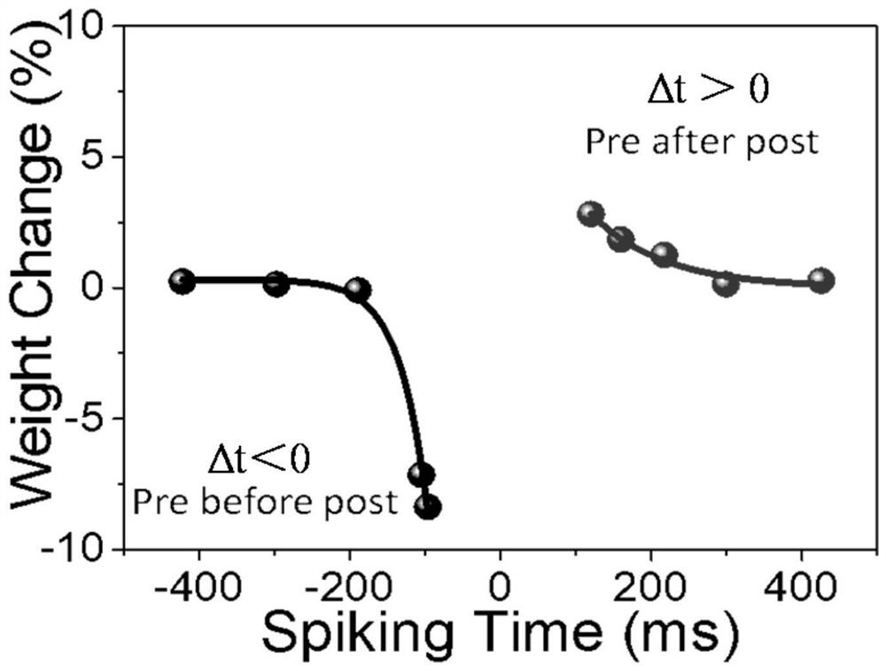
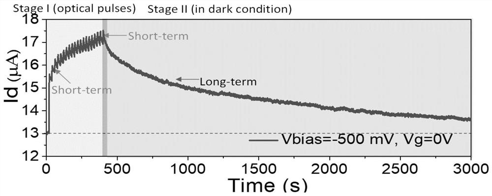
[0028] The invention proposes a method for simulating the optical synapse of a living body. The method generates an optical signal used to simulate the action potential of the front end of the synapse in the living body, and utilizes the space generated by the semiconductor photosensitive material that responds to the optical signal. The hole-electron pairs move directionally under the electric field, thereby changing the concentration of carriers in the post-synaptic terminal, and then increasing or decreasing the current passing through the post-synaptic terminal, so as to simulate the basic performance of biological synapses under the stimulation of light signals.

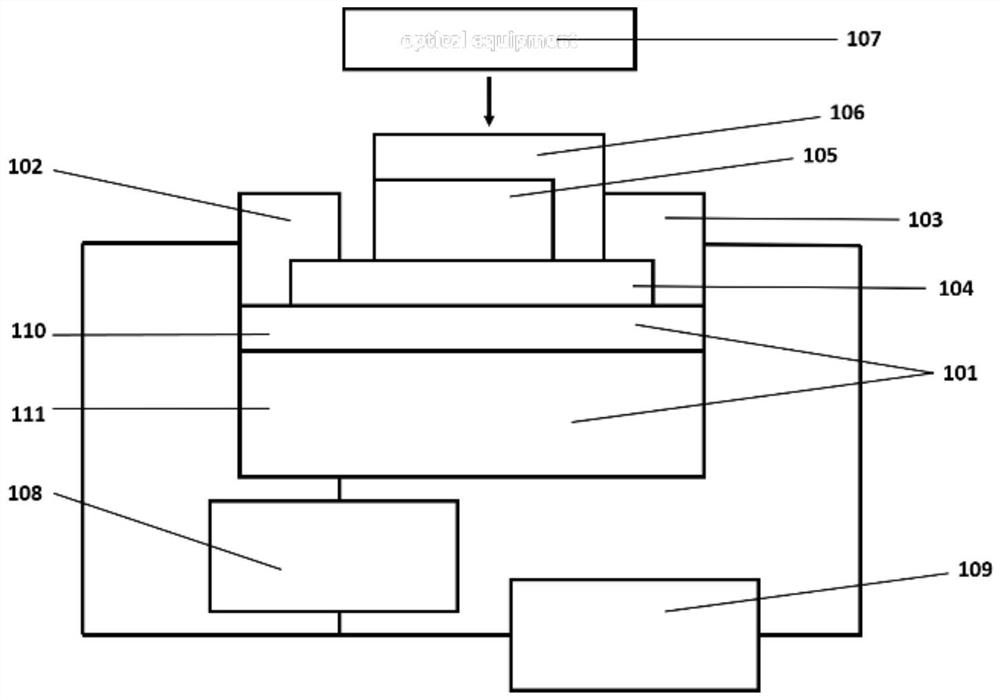
[0029] The present invention also proposes an optical synapse device based on the above method, and its overall structure ca...


PUM


Abstract

A method and device for simulating biological optical synapse proposed by the invention belong to the technical field of bionic synapse. In this method, an optical signal used to simulate the action potential of the front end of the synapse in a living body is generated, and the hole-electron pair generated by the semiconductor photosensitive material that responds to the optical signal is used to move directionally under the electric field, thereby changing the post-synaptic The concentration of carriers in the terminal increases or decreases the current through the postsynaptic terminal, so as to simulate the basic performance of biological synapses under the stimulation of light signals. The device includes a substrate, a first electrode, a second electrode, a post-synaptic layer, a semiconductor photosensitive layer, a pre-synaptic layer, a light source signal input device, a back gate signal input device and a source-drain signal input device. The invention realizes the basic performance of simulating biological synapse under optical signal stimulation, can greatly reduce the power consumption caused by the existence of the bus, and makes it possible to directly convert optical images into synaptic weights and bring them into artificial neural networks for image recognition. possible.

Description

technical field [0001] The invention belongs to the technical field of bionic synapse, in particular to a method and device for simulating biological optical synapse. Background technique [0002] Since the 21st century, with the continuous reduction of the physical size of the integrated circuit process, the performance has also been rapidly improved. The emergence of Alpha Dog has also brought artificial intelligence to an upsurge. However, the huge power consumption behind AlphaGo has also drawn people's attention to the problems that exist in the von Neumann structure of traditional computers. Furthermore, when comparing the power consumption of AlphaGo and Li Shishi when dealing with the same Go problem, people also found the huge advantage of the human brain in processing information with low power consumption. Therefore, bionic electronic devices have also attracted widespread attention. [0003] At present, the reason for the huge power consumption of the current h...

Claims


Application Information

Patent Timeline
Patent Type & Authority Patents(China)
IPC IPC(8): G06N3/067
CPCG06N3/0675
Inventor 任天令田禾吴凡王雪峰杨轶
Owner TSINGHUA UNIV
Why Eureka
Try Eureka