Eureka AIR delivers breakthrough ideas for toughest innovation challenges, trusted by R&D personnel around the world.

Pixel compensation method and device, storage medium, and display screen

A compensation method and display technology, applied to static indicators, cathode ray tube indicators, instruments, etc., can solve the problems of OLED display aging, OLED display uniformity decline, OLED display screen uniformity, etc.

Active Publication Date: 2019-03-26
BOE TECH GRP CO LTD
View PDF8 Cites 15 Cited by
  • Summary
  • Abstract
  • Description
  • Claims
  • Application Information

AI Technical Summary

Problems solved by technology

[0004] However, the organic light-emitting layer in the OLED display will gradually age as the use time increases, making the OLED display aging, and the uniformity of the displayed picture of the aged OLED display will decrease. The above pixel compensation method can only be used in OLED Pixel compensation is performed before the display leaves the factory, so it cannot compensate for the pixel aging of the OLED display, resulting in low uniformity of the picture displayed on the OLED display

Method used


Image

  • Pixel compensation method and device, storage medium, and display screen
  • Pixel compensation method and device, storage medium, and display screen
  • Pixel compensation method and device, storage medium, and display screen

Examples


Embodiment Construction

[0129] In order to make the object, technical solution and advantages of the present invention clearer, the present invention will be further described in detail below in conjunction with the accompanying drawings. Obviously, the described embodiments are only some embodiments of the present invention, rather than all embodiments . Based on the embodiments of the present invention, all other embodiments obtained by persons of ordinary skill in the art without making creative efforts belong to the protection scope of the present invention.

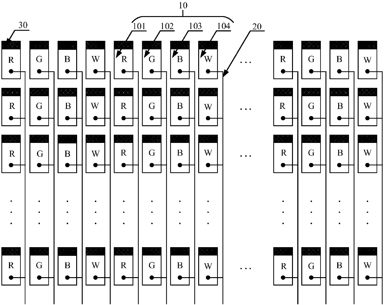
[0130] Please refer to figure 1 , figure 1 The front view of the display screen provided for the embodiment of the present invention, the display screen can be an OLED display screen or a quantum dot light emitting diode (Quantum Dot Light Emitting Diodes, QLED) display screen, and the display screen includes a plurality of pixels arranged in a matrix 10. Each pixel 10 includes a plurality of sub-pixels, and the sub-pixels on the display ...


PUM


Abstract

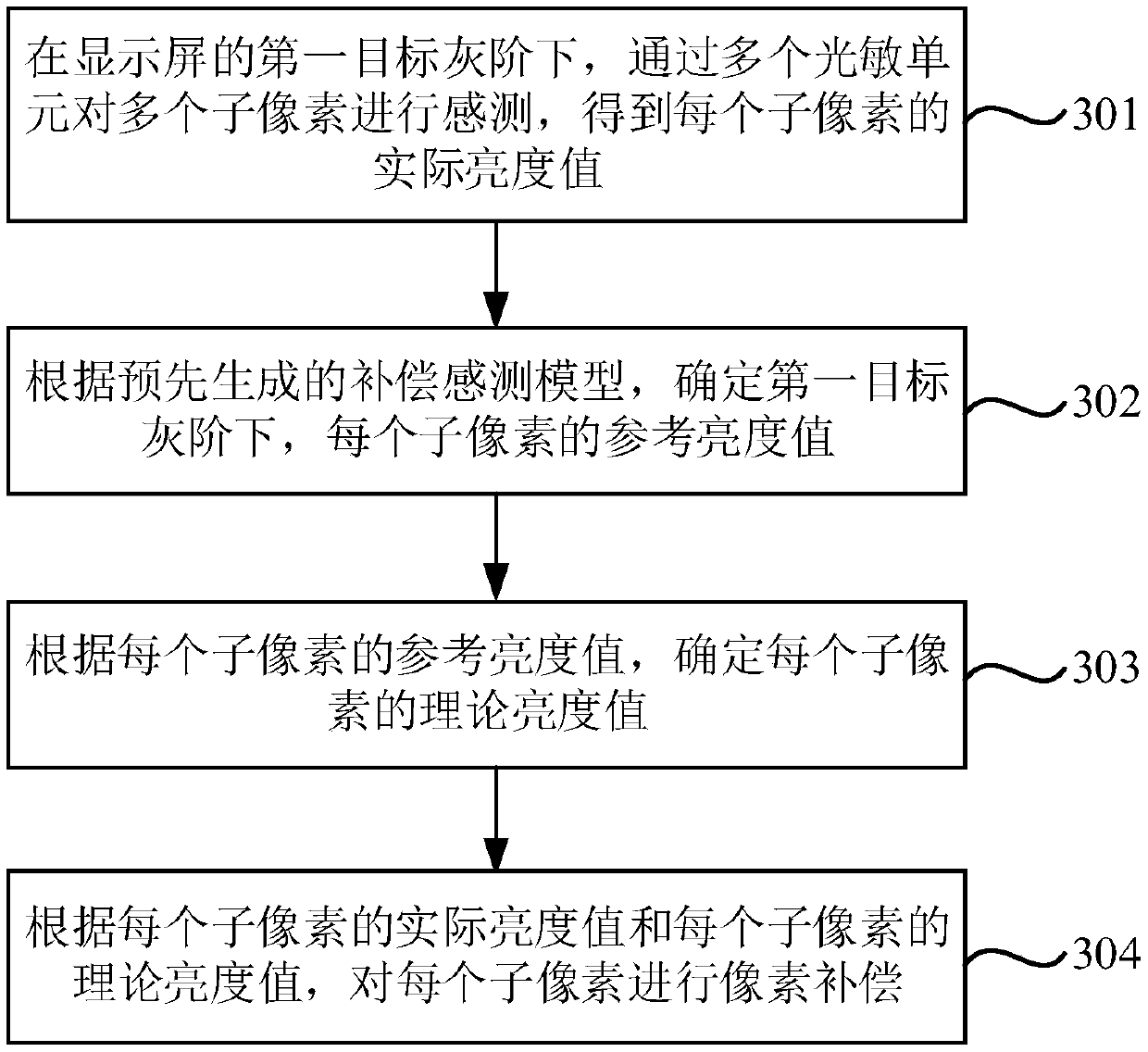
The invention relates to a pixel compensation method and device, a storage medium and a display screen, and belongs to the technical field of display. The method includes the steps: sensing a plurality of sub-pixels by using a plurality of photosensitive cells at a first target gray scale of the display screen to obtain an actual brightness value of each sub-pixel; determining a reference luminance value of each sub-pixel at the first target gray scale according to a pre-generated compensation sensing model, wherein the compensation sensing model is used to record the correspondence relation between the target gray scale and theoretical pixel data, and the theoretical pixel data includes the reference luminance value of each sub-pixel; determining the theoretical luminance value of each sub-pixel according to the reference luminance value of each sub-pixel; and performing pixel compensation for each sub-pixel according to the actual luminance value of each sub-pixel and the theoreticalluminance value of each sub-pixel. The method realizes the compensation for the pixel aging of the display screen, and improves the uniformity of an image displayed on the display screen. The methodis used to compensate for the display screen.

Description

technical field [0001] The invention relates to the field of display technology, in particular to a pixel compensation method and device, a storage medium, and a display screen. Background technique [0002] With the development of display technology, organic light emitting diode (Organic Light Emitting Diode, OLED) display screen is more and more used in high-performance display products because of its characteristics such as self-illumination, fast response, and wide viewing angle. In order to ensure the quality of the OLED display screen, it is necessary to perform pixel compensation on the OLED display screen to improve the uniformity of the displayed image. [0003] The current pixel compensation method is usually an optical compensation method. The compensation process is: before the OLED display leaves the factory, light up the OLED display with each of the multiple characteristic grayscales, and light up the OLED display with each characteristic grayscale. After lig...

Claims


Application Information

Patent Timeline
IPC IPC(8): G09G3/3225
CPCG09G3/3225G09G2320/0233G09G3/3208G09G3/2074G09G2320/045G09G2360/144G09G2360/147G09G2360/145G09G5/10G09G2320/0271G09G2360/141
Inventor 朱明毅林奕呈
Owner BOE TECH GRP CO LTD
Why Eureka
Eureka Blog
Learn More