Tunneling field effect transistor

A tunneling field effect, transistor technology, applied in semiconductor devices, electrical components, circuits, etc., can solve the problems of reducing power consumption and inability to achieve, and achieves increasing on-state current, reducing tunneling distance, and increasing energy band. The effect of overlapping areas

Active Publication Date: 2019-04-02
NANTONG UNIVERSITY
View PDF2 Cites 0 Cited by
  • Summary
  • Abstract
  • Description
  • Claims
  • Application Information

AI Technical Summary

Problems solved by technology

[0002] With the continuous shrinking of the feature size of semiconductor devices, Metal Oxide Semiconductor Field Effect Transistor (MOSFET) devices are limited by the sub-threshold swing limit (60mV / dec), high off-state current, short channel effect, etc., reducing the operating voltage will Cannot achieve the effect of reducing power consumption

Method used


Image

  • Tunneling field effect transistor
  • Tunneling field effect transistor
  • Tunneling field effect transistor

Examples


Embodiment Construction

[0017] In order to facilitate the understanding of the present invention, the present invention will be described more fully below with reference to the associated drawings. Typical embodiments of the invention are shown in the drawings. However, the present invention can be embodied in many different forms and is not limited to the embodiments described herein. Rather, these embodiments are provided so that the disclosure of the present invention will be thorough and complete.

[0018] It should be noted that when an element is referred to as being “fixed” to another element, it can be directly on the other element or there can also be an intervening element. When an element is referred to as being "connected to" another element, it can be directly connected to the other element or intervening elements may also be present. The terms "left", "right" and similar expressions are used herein for the purpose of illustration only.

[0019] Unless otherwise defined, all technical...


PUM


Abstract

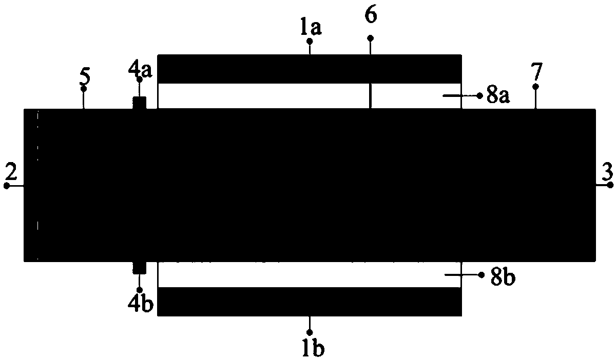
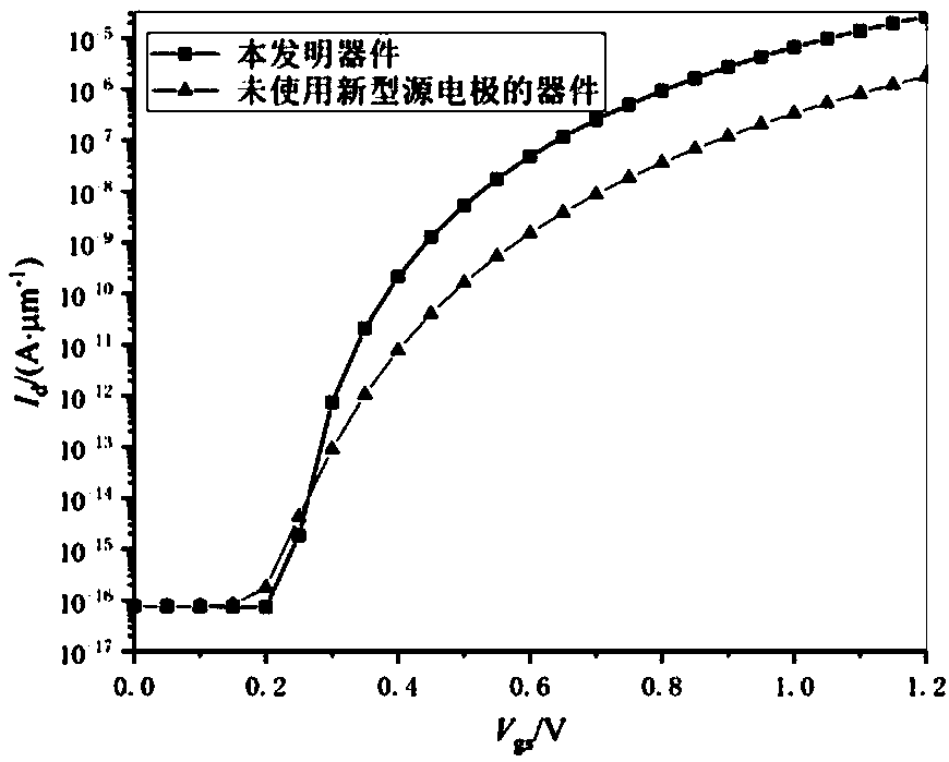
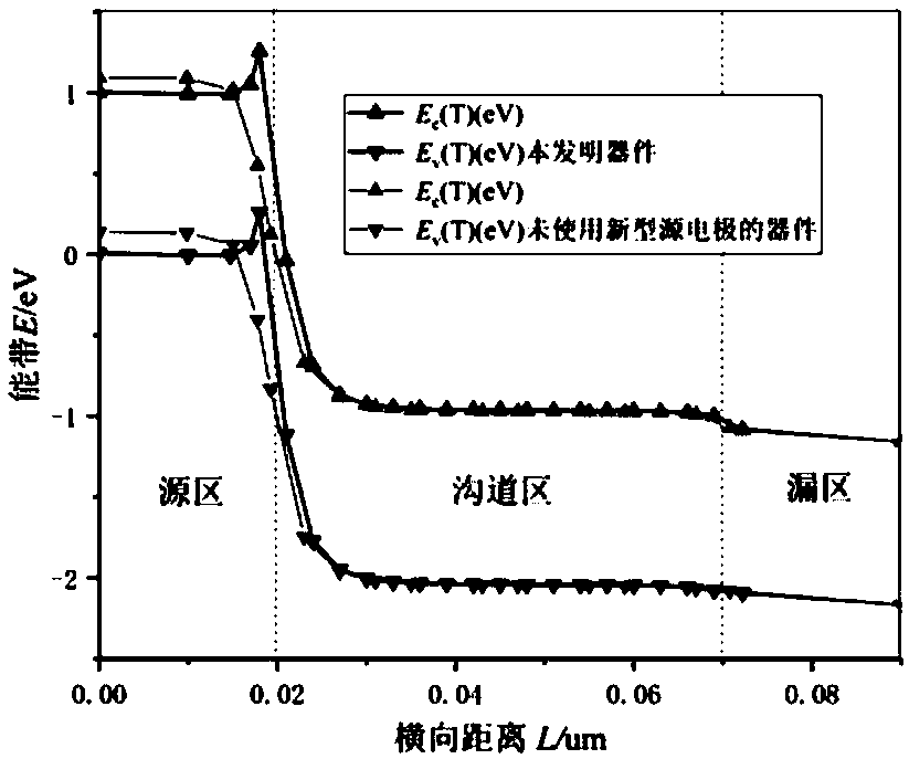
The invention discloses a tunneling field effect transistor. The tunneling field effect transistor comprises a source region, a channel region and a drain region which are connected among a gate electrode, a source electrode and a drain electrode, the source region and the drain region are partitioned through the channel region, the source electrode is an ohmic contact electrode and is in ohmic contact with the source region, and the drain electrode is an ohmic contact electrode and is in ohmic contact with the drain region. The transistor also comprises a metallic first schottky electrode arranged in a floating manner, the first schottky electrode is in schottky contact with the source region, and the first schottky electrode is arranged at the position of a contact surface close to the part between the source region and the channel region. According to the tunneling field effect transistor, a novel source electrode structure composed of the schottky electrode and the source electrodeis designed on the basis of a traditional TFET device, the metallic floating schottky contact electrode with high work function can effectively raise an energy band under the schottky contact electrode effectively, the overlay region of the energy band between a valence band in the source region and a conduction band in the channel region is increased, the tunneling distance is reduced, and the ON state current is improved.

Description

technical field [0001] The invention relates to the field of semiconductor devices, in particular to a tunneling field effect transistor. Background technique [0002] With the continuous shrinking of the feature size of semiconductor devices, Metal Oxide Semiconductor Field Effect Transistor (MOSFET) devices are limited by the sub-threshold swing limit (60mV / dec), high off-state current, short channel effect, etc., reducing the operating voltage will The effect of reducing power consumption cannot be achieved. Since the tunneling field-effect transistor (Tunneling field-effect transistor, TFET) works on the physical mechanism of band-band tunneling, it has lower sub-threshold swing and off-state current, so it is regarded as the most suitable nanoscale MOSFET. One of the strong contenders. However, the low on-state current of TFET greatly limits its application, so how to increase the on-state current of TFET is an urgent problem to be solved. [0003] At present, in ord...

Claims


Application Information

Patent Timeline
IPC IPC(8): H01L29/739H01L29/417H01L29/47
CPCH01L29/41725H01L29/47H01L29/7391
Inventor 施敏柯亚威张威朱友华
Owner NANTONG UNIVERSITY
Why Eureka
Try Eureka