

Exposure apparatus, exposure method, and device manufacturing method
A technology of exposure device and light source, applied in the field of lithography system and process, can solve the problem of lithography equipment being unable to switch modes and the like
- Summary
- Abstract
- Description
- Claims
- Application Information
AI Technical Summary
Problems solved by technology
Method used
Image

Examples
Embodiment Construction
[0032] The exposure device proposed by the present invention will be described in further detail below in conjunction with the accompanying drawings and specific embodiments. The advantages and features of the present invention will become clearer from the following description. It should be noted that all the drawings are in a very simplified form and use imprecise scales, and are only used to facilitate and clearly assist the purpose of illustrating the embodiments of the present invention.
[0033] This embodiment provides a specific implementation of the exposure device.
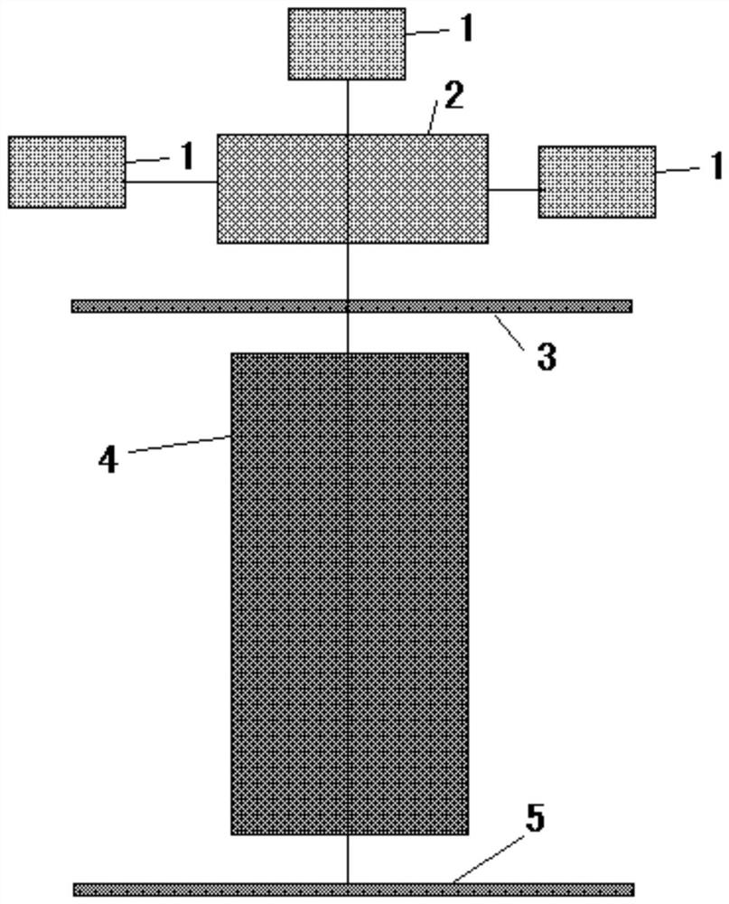
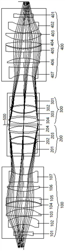
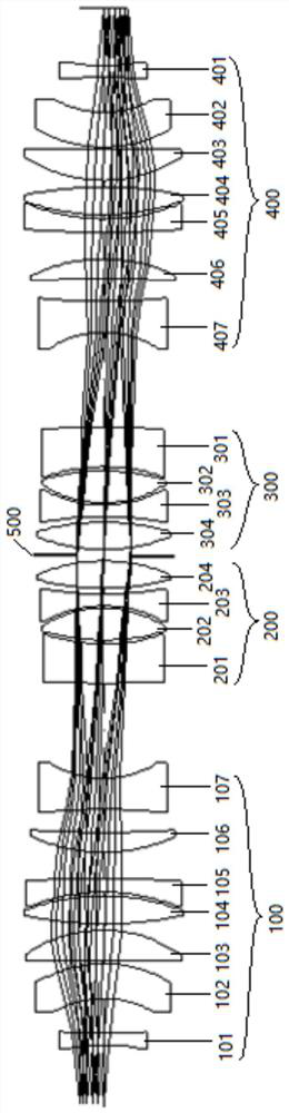
[0034] figure 1 It is a schematic diagram of the connection relationship of an exposure device provided in the embodiment of the present invention; figure 2 It is a structural schematic diagram and a schematic optical path diagram of an optical lens module under the first numerical aperture in Embodiment 1 of the present invention; image 3 It is a structural schematic diagram and a schematic optical...
PUM
| Property | Measurement | Unit |
|---|---|---|
| refractive index | aaaaa | aaaaa |
Abstract
Description
Claims
Application Information