A b-doped nisi/n-si photoanode and its preparation method and application

A photoanode, n-si technology, which is applied in the field of photoelectrochemistry, can solve the problems of blocking photogenerated charges, low photocurrent density, and reducing the performance of photoanode, and achieves the effect of avoiding the blocking effect.

Active Publication Date: 2021-03-30
TECHNICAL INST OF PHYSICS & CHEMISTRY - CHINESE ACAD OF SCI +2
View PDF5 Cites 0 Cited by
  • Summary
  • Abstract
  • Description
  • Claims
  • Application Information

AI Technical Summary

Problems solved by technology

Although the introduction of an insulating layer can effectively reduce the density of interface states and increase the height of the Schottky barrier, this layer of insulating layer will block the transport of photogenerated charges resulting in low photocurrent density.
In addition, this metal-insulator-silicon composite structure cannot avoid the natural SiO on the Si surface. 2 layer, this layer of natural SiO 2 layer brings a poor Si / SiO 2 The interface severely degrades the performance of the photoanode

Method used


Image

  • A b-doped nisi/n-si photoanode and its preparation method and application
  • A b-doped nisi/n-si photoanode and its preparation method and application
  • A b-doped nisi/n-si photoanode and its preparation method and application

Examples


Embodiment 1

[0039] This embodiment provides a method for preparing a NiSi / n-Si photoanode, the specific method is:

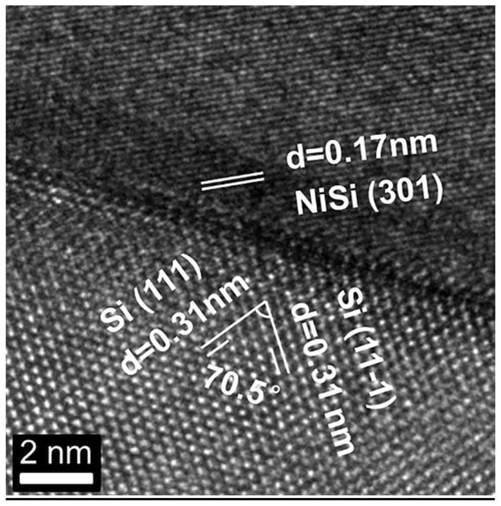
[0040] (1) The p-doped n-type silicon wafer with a resistivity of 1-10Ω·cm is cleaned by a standard RCA method. Soak the cleaned silicon wafer in 10% dilute HF solution for 10 seconds to remove the surface oxide layer. The silicon wafer from which the surface oxide layer has been removed is immediately put into a magnetron sputtering chamber, and a Ni film with a thickness of 7 nm is deposited on it by magnetron sputtering to obtain a Ni / n-Si structure.

[0041] (2) Put the Ni / n-Si structure obtained in step (1) into a rapid heat treatment furnace, 2 Under atmosphere, rapid heat treatment at 500° C. for 30 seconds to obtain a NiSi / n-Si structure.

[0042] (3) Put the NiSi / n-Si structure obtained in step (2) into an ion implanter for ion implantation, the implanted ions are boron ions, and the implantation dose is 1×10 15 -5×10 15 cm -2 .

[0043] (4) Put the NiSi / n-Si...

Embodiment 2

[0049] This embodiment provides a method for preparing a NiSi / n-Si photoanode, the specific method is:

[0050] (1) The p-doped n-type silicon wafer with a resistivity of 1-10Ω·cm is cleaned by a standard RCA method. Soak the cleaned silicon wafer in 10% dilute HF solution for 10 seconds to remove the surface oxide layer. The silicon wafer from which the surface oxide layer has been removed is immediately put into a magnetron sputtering chamber, and a Ni film with a thickness of 7 nm is deposited on it by magnetron sputtering to obtain a Ni / n-Si structure.

[0051] (2) Put the Ni / n-Si structure obtained in step (1) into a rapid heat treatment furnace, 2 Under atmosphere, rapid heat treatment at 500° C. for 30 seconds to obtain a NiSi / n-Si structure.

[0052] (3) Put the NiSi / n-Si structure obtained in step (2) into an ion implanter for ion implantation, the implanted ions are boron ions, and the implantation dose is 1×10 15 -5×10 15 cm -2 .

[0053] (4) Put the NiSi / n-Si...


PUM

PropertyMeasurementUnit
thicknessaaaaaaaaaa
thicknessaaaaaaaaaa
electrical resistivityaaaaaaaaaa

Abstract

The invention provides a B-doped NiSi / n-Si photoanode, comprising an n type monocrystalline silicon piece, a B-doped NiSi thin film generated on the surface of the n type monocrystalline silicon piecein situ by virtue of solid-phase reaction, and a SiO2 layer does not exist between the n type monocrystalline silicon piece of the photoanode and the B-doped NiSi thin film. Therefore, the NiSi / n-Siphotoanode structure provided by the invention is very beneficial to transmission of photoinduced charges, and saturation photocurrent density of the photoanode under the AM1.5 sunlight illumination condition can reach 33mA / cm<2>. Besides, the photoanode provided by the invention is doped with B, and a rapid heat treatment process is performed in a preparation process, so that the photoanode has avery high Schottky barrier, a high photovoltage can be produced, and then an opening potential is effectively reduced to 1.03V vs RHE. Besides, the invention also provides a preparation method of thephotoanode and application of the photoanode in photoelectrochemical water decomposition.

Description

technical field [0001] The invention relates to the technical field of photoelectrochemistry. More specifically, it relates to a B-doped NiSi / n-Si photoanode and its preparation method and application. Background technique [0002] Photoelectrochemical water splitting is considered to be an effective means to realize the conversion of solar energy to hydrogen energy. Si is considered as an ideal photoanode material due to its abundant content in the earth's crust, suitable energy level position, and high carrier mobility. The problem facing Si as a photoanode material is that the anode corrosion of Si and the kinetic process of oxygen generation reaction on the Si surface are very slow. Depositing a layer of metal with oxygen-generating catalytic activity on Si can not only protect Si from corrosion, but also greatly increase the rate of oxygen-generating reaction. However, when the metal is directly deposited on the Si surface, a large number of interface states will be ...

Claims


Application Information

Patent Timeline
Patent Type & Authority Patents(China)
IPC IPC(8): H01L31/0224H01L31/18
CPCY02P70/50
Inventor 师文生李生阳罗军佘广为许静
Owner TECHNICAL INST OF PHYSICS & CHEMISTRY - CHINESE ACAD OF SCI
Why Eureka
Try Eureka