
Array substrate and display device

An array substrate and projection technology, which is used in static indicators, instruments, electrical components, etc., can solve the problems of small number of pixels and signal lines occupying a lot of space, and achieve the effect of reducing area, improving display quality, and saving wiring space.

Inactive Publication Date: 2019-07-26
HEFEI BOE ZHUOYIN TECH CO LTD +1
View PDF8 Cites 15 Cited by
  • Summary
  • Abstract
  • Description
  • Claims
  • Application Information

AI Technical Summary

Problems solved by technology

[0005] The purpose of the present disclosure is to provide an array substrate and a display device, and then at least to a certain extent overcome the problem that the number of pixels per unit area in the pixel region is small due to the signal lines occupying a large amount of space in the related art

Method used


Image

  • Array substrate and display device
  • Array substrate and display device
  • Array substrate and display device

Examples


Embodiment Construction

[0057]Example embodiments will now be described more fully with reference to the accompanying drawings. Example embodiments may, however, be embodied in many forms and should not be construed as limited to the embodiments set forth herein; rather, these embodiments are provided so that this disclosure will be thorough and complete, and will fully convey the concept of example embodiments to those skilled in the art. The same reference numerals in the drawings denote the same or similar structures, and thus their detailed descriptions will be omitted.

[0058] Although relative terms such as "upper" and "lower" are used in this specification to describe the relative relationship of one component of an icon to another component, these terms are used in this specification only for convenience, for example, according to the description in the accompanying drawings directions for the example described above. It will be appreciated that if the illustrated device is turned over so ...


PUM


Abstract

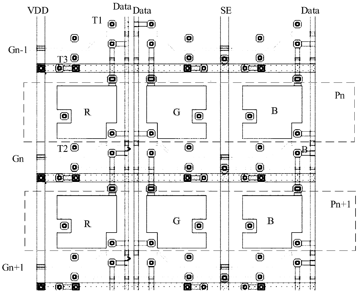
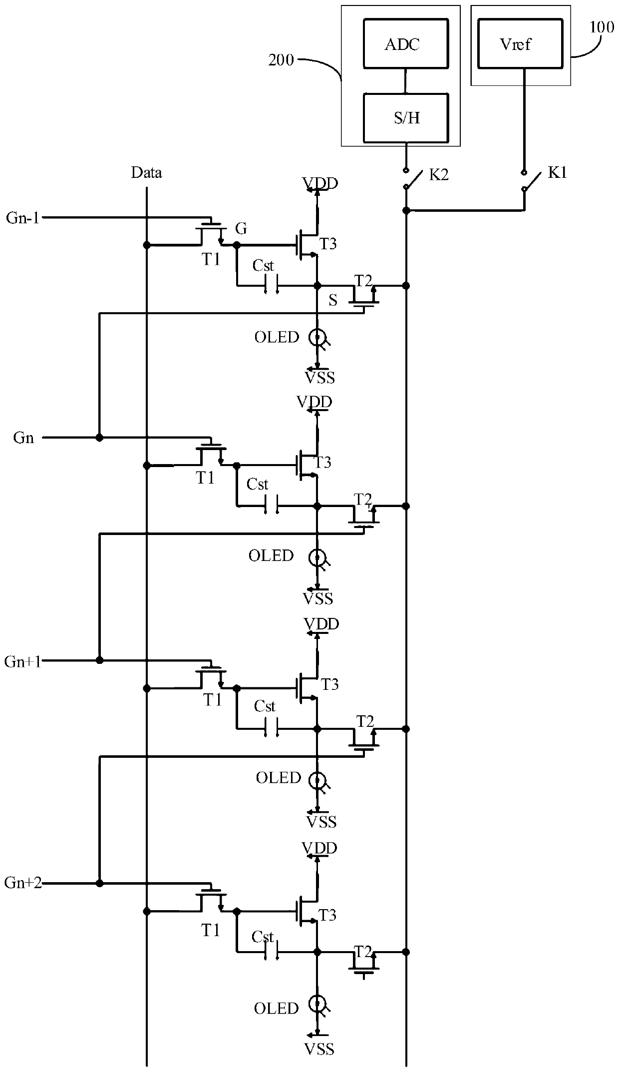
The invention relates to an array substrate and a display device. The array substrate comprises a substrate, a driving circuit and N rows of light emitting units, wherein the driving circuit is arranged on the substrate; the N rows of light-emitting units are arranged on one side, far away from the substrate, of the driving circuit; the driving circuit comprises N rows of driving circuit units anda plurality of first scanning signal lines; the projection of one of the first scanning signal lines on the substrate is located in a first area, wherein the first area is the area between the projection of the first row of light emitting unit of any two adjacent rows of light emitting units in the N rows of light emitting units on the substrate and the projection of the second row of light emitting unit on the substrate; and the grid electrode of a second transistor of the first row driving circuit and the grid electrode of a first transistor of the second row driving circuit are connected to the corresponding first scanning signal lines.

Description

technical field [0001] The present disclosure relates to the field of display technology, and in particular, to an array substrate and a display device. Background technique [0002] With the development and progress of technology, OLED display devices have been widely used in various electronic products, and electronic products have higher and higher requirements on the display quality and screen ratio of display devices. In a display device, a driving circuit is usually used to drive pixel units to emit light to display images. The driving circuit includes a large number of signal lines, such as source lines and gate lines. [0003] A large number of signal lines in the driving circuit require more wiring space, which reduces the space for arranging pixel units in the array substrate, reduces the number of pixels per unit area in the pixel region, and affects display quality. [0004] It should be noted that the information disclosed in the above background section is onl...

Claims


Application Information

Patent Timeline
Patent Type & Authority Applications(China)
IPC IPC(8): H01L27/32G09G3/3225
CPCG09G3/3225H10K59/12H10K59/1213H10K59/131G09G3/3233G09G3/3266G09G2310/0286
Inventor 冯雪欢吴思翔
Owner HEFEI BOE ZHUOYIN TECH CO LTD
Learn More