
Image sensor and manufacturing method thereof

A technology of image sensor and manufacturing method, which is applied in the direction of electric solid-state devices, semiconductor devices, radiation control devices, etc., can solve the problems of light crosstalk, affecting image quality, entering, etc., and achieve the effect of preventing crosstalk and improving image quality

Inactive Publication Date: 2019-08-06
HUAIAN IMAGING DEVICE MFGR CORP
View PDF7 Cites 5 Cited by
  • Summary
  • Abstract
  • Description
  • Claims
  • Application Information

AI Technical Summary

Problems solved by technology

However, sometimes the light passing through the color filter layer will enter the adjacent photoelectric conversion region due to the incident angle, resulting in light crosstalk and affecting image quality. Therefore, the structure of the image sensor that can better prevent light crosstalk has been being explored.

Method used


Image

  • Image sensor and manufacturing method thereof
  • Image sensor and manufacturing method thereof
  • Image sensor and manufacturing method thereof

Examples


Embodiment Construction

[0025] The following description provides specific application scenarios and requirements of the application, with the purpose of enabling those skilled in the art to manufacture and use the contents of the application. Various local modifications to the disclosed embodiments will be readily apparent to those skilled in the art, and the general principles defined herein may be applied to other embodiments and embodiments without departing from the spirit and scope of the disclosure. application. Thus, the present disclosure is not limited to the embodiments shown, but is to be accorded the widest scope consistent with the claims.

[0026] The technical solution of the present invention will be described in detail below in conjunction with the embodiments and the accompanying drawings.

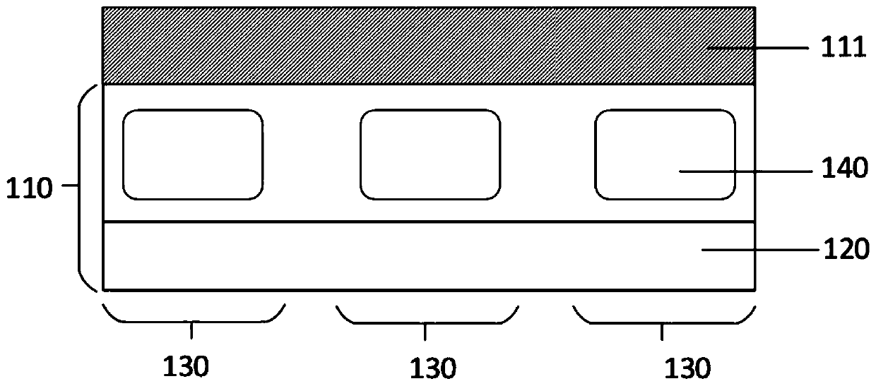
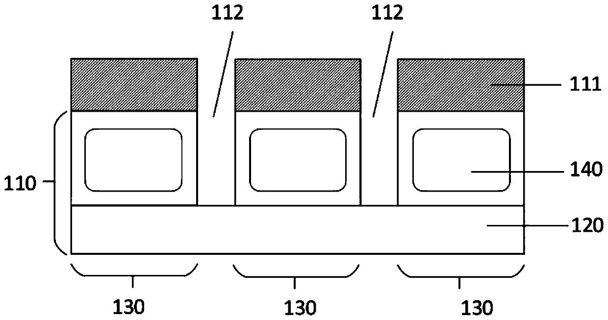
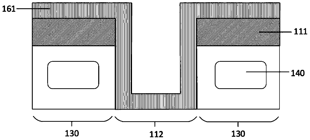
[0027] This embodiment provides a method for fabricating an image sensor, including: providing a semiconductor substrate 110, the semiconductor substrate 110 including more than one photoelect...


PUM


Abstract

The application relates to an image sensor and a manufacturing method thereof. The manufacturing method of the image sensor comprises the following steps: providing a semiconductor substrate, whereinthe semiconductor substrate includes more than one photoelectric conversion area, and a photosensitive element is formed in each of the more than one photoelectric conversion area; forming a mask layer on the semiconductor substrate, and forming deep grooves in the mask layer and between any adjacent photoelectric conversion areas among the more than one photoelectric conversion area; filling thedeep grooves with optical waveguide structures; removing the mask layer; and forming color filter layers above the photoelectric conversion areas, wherein the optical waveguide structures isolate anyadjacent photoelectric conversion areas among the more than one photoelectric conversion area and the adjacent color filter layers and prevent the crosstalk of light in the adjacent photoelectric conversion areas, thus improving the image quality.

Description

technical field [0001] The invention relates to the field of manufacturing semiconductor devices, in particular to an image sensor and a manufacturing method thereof. Background technique [0002] At present, CMOS image sensors have two structures: front-illuminated image sensor and back-illuminated image sensor. The front-illuminated image sensor is a structure in which light passes through the metal wiring layer to the photoelectric conversion area for sensing light, while the back-illuminated image sensor places the photoelectric conversion area above the metal wiring layer so that the light does not need to pass through the metal wiring layer. A structure that can reach the photoelectric conversion region for sensing light. The back-illuminated image sensor has higher photoelectric conversion efficiency than the front-illuminated image sensor, so the back-illuminated image sensor has been more widely used. [0003] In the back-illuminated image sensor, the light is gat...

Claims


Application Information

Patent Timeline
Patent Type & Authority Applications(China)
IPC IPC(8): H01L27/146
CPCH01L27/14621H01L27/14623H01L27/14629H01L27/1463H01L27/1464H01L27/14685
Inventor 赵培培吴明林宗贤吴龙江孙明亮马亚辉
Owner HUAIAN IMAGING DEVICE MFGR CORP
Learn More