Color filter substrate, manufacturing method thereof, and OLED display device
a technology of color filter substrate and manufacturing method, applied in semiconductor devices, diodes, instruments, etc., can solve the problems of high visibility and brightness of display substrate, affecting display effect, etc., to prevent color mixing, improve display effect, and prevent light crosstalk
- Summary
- Abstract
- Description
- Claims
- Application Information
AI Technical Summary
Benefits of technology
Problems solved by technology
Method used
Image
Examples
embodiment 1
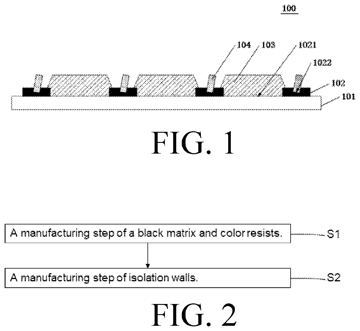
[0028]As shown in FIG. 1, a color filter substrate comprises a substrate 101, a black matrix 102, a plurality of color resists 103, and a plurality of isolation walls 104. Wherein, the black matrix 102 is disposed on the substrate 101, and the black matrix 102 is provided with a plurality of openings 1021 arranged at intervals in a matrix. The color resists 103 are coated in the openings 1021. Wherein, a plurality of grooves 1022 are disposed on the black matrix 102 and between two of the adjacent color resists 103, and the isolation walls 104 are disposed on the grooves 1022.
[0029]Wherein, the grooves 1022 may be one or more of rectangular grooves, serrated grooves, wavy grooves, and arc-shaped grooves. The grooves 1022 in the embodiment are rectangular grooves. Since black polyimide materials have certain fluidity, it is easy to position the isolation walls 104 by disposing the grooves.
[0030]Wherein, a constituent material of the isolation walls 104 comprises a black polyimide (PI...
embodiment 2
[0032]As shown in FIG. 2, an embodiment provides a manufacturing method of a color filter substrate of the present disclosure. The method comprises step S1: a manufacturing step of a black matrix and color resists, specifically, providing the substrate 101, manufacturing the black matrix 102 on the substrate 101 by coating, baking, exposing, and developing processes, arranging the openings at intervals in a matrix on the black matrix 102, and disposing the color resists 103 in the openings; and step S2: a manufacturing step of isolation walls, specifically, manufacturing a plurality of grooves 1022 on the black matrix 102 and between the adjacent color resists 103, then printing or coating an isolation wall material containing a black PI material on the grooves 1022, irradiating the isolation wall material by ultraviolet light, and making the isolation wall material form the isolation walls 104 on the black matrix 102.
embodiment 3
[0033]The embodiment of the present disclosure provides an OLED display device which comprises the color filter substrate 100 of the present disclosure and an OLED device 200. The color filter substrate 100 is disposed on the OLED device 200.
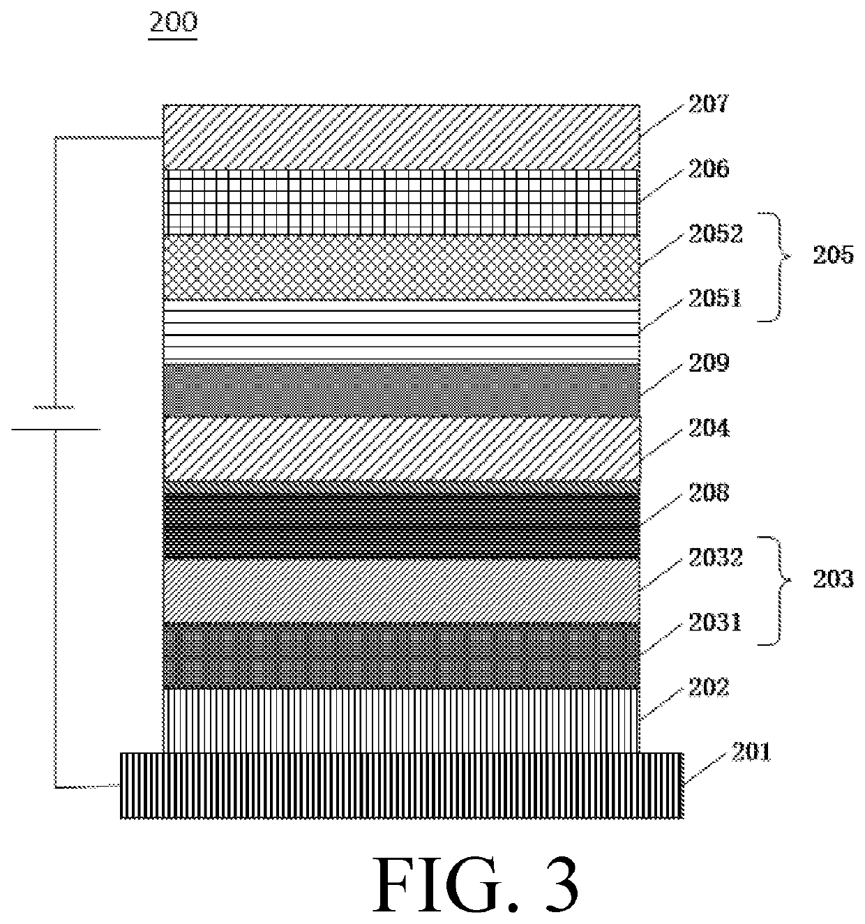
[0034]As shown in FIG. 3, the OLED device 200 comprises a substrate base 201, an anode layer 202, a first functional layer 203, an organic light-emitting layer 204, a second functional layer 205, a cathode layer 206, and a light extraction layer 207. The anode layer 202 is disposed on the substrate base 201, the first functional layer 203 is disposed on the anode layer 202, the organic light-emitting layer 204 is disposed on the first functional layer 203, the second functional layer 205 is disposed on the organic light-emitting layer 204, the cathode layer 206 is disposed on the second functional layer 205, and the light extraction layer 207 is disposed on the cathode layer 206.
[0035]The substrate base 201 can be glass or a TFT backboard. The T...
PUM
| Property | Measurement | Unit |
|---|---|---|
| brightness | aaaaa | aaaaa |
| power saving | aaaaa | aaaaa |
| voltage | aaaaa | aaaaa |
Abstract
Description
Claims
Application Information

