Method for preparing backside-illuminated sensor
A sensor and back-illuminated technology, which is applied in the field of back-illuminated sensor preparation, can solve problems affecting the performance of back-illuminated sensor chips, crosstalk, and abnormal protrusions formed on the metal grid layer, so as to avoid abnormal protrusions and reduce abnormalities. Growth, avoiding the effect of light crosstalk
- Summary
- Abstract
- Description
- Claims
- Application Information
AI Technical Summary
Problems solved by technology
Method used
Image
Examples
Embodiment 1
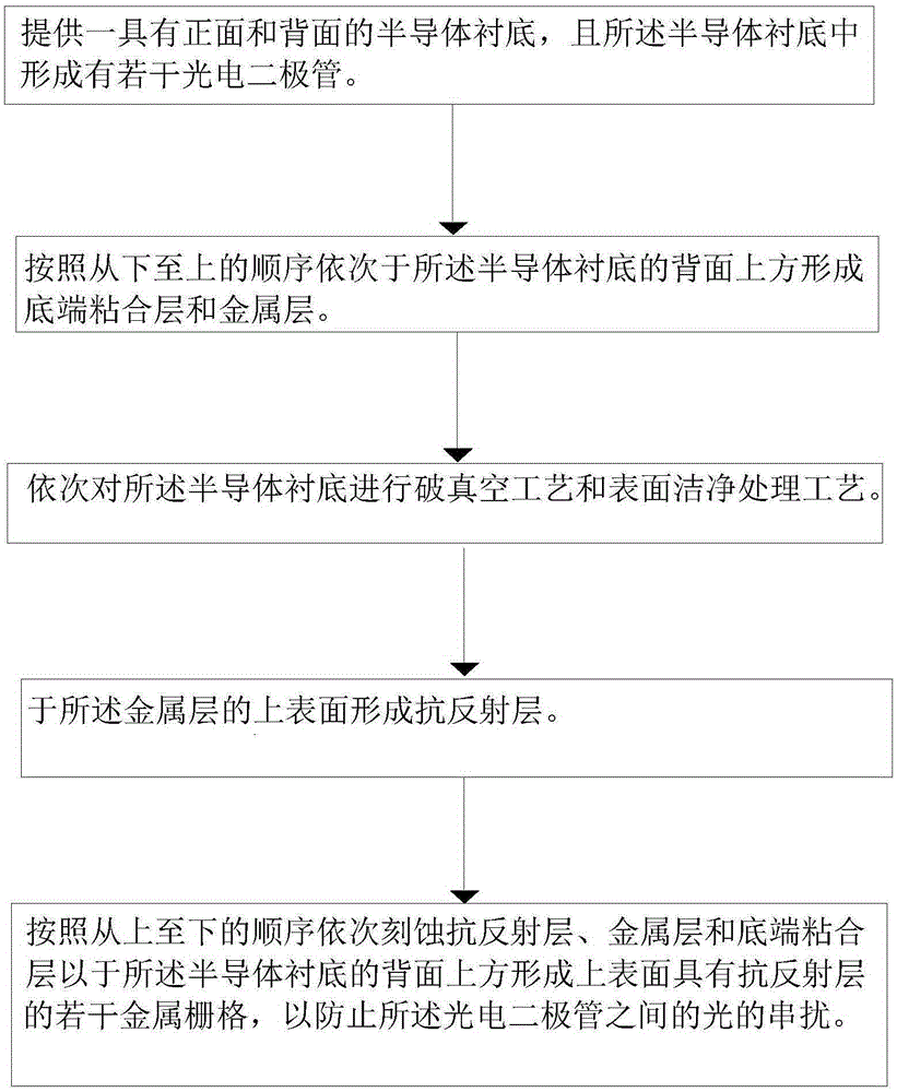
[0027] Such as figure 1 As shown, this embodiment relates to a method for preparing a back-illuminated sensor, which may be a back-illuminated image sensor. Specifically, the method includes the following steps:
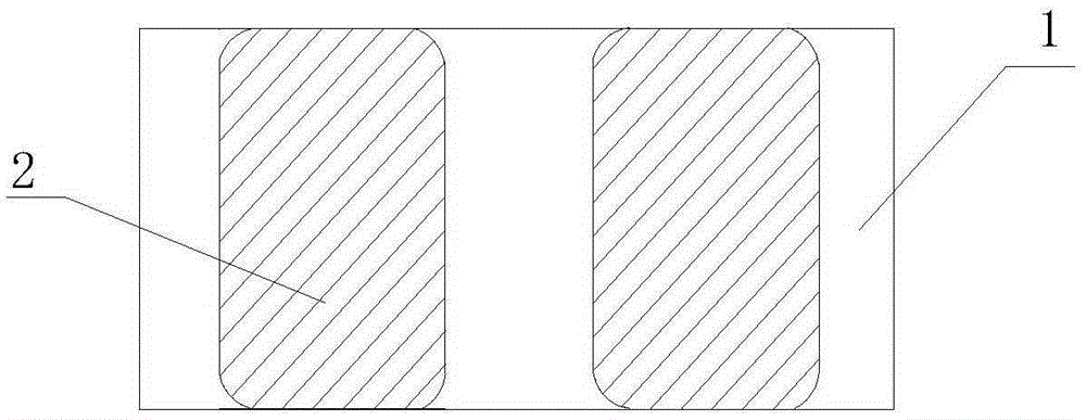
[0028] Step 1, providing a semiconductor substrate 1 with a front and a back surface, and a photodiode array (pixel array) formed by several photodiodes 2 (pixels) is formed in the semiconductor substrate 1; in an embodiment of the present invention, the Semiconductor substrate 1 is the wafer that has finished the previous layer process; figure 2 structure shown.
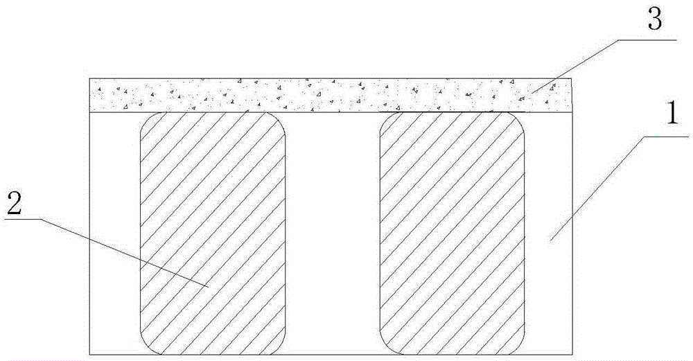
[0029] Step 2, forming a bottom adhesive layer 3 on the back surface of the semiconductor substrate 1; Ion sputtering machine is formed by physical ion sputtering. Preferably, the material of the bottom bonding layer 3 is titanium nitride; as image 3 structure shown.
[0030] Step 3, forming a metal layer 4 on the upper surface of the bottom adhesive layer 3; in an embodiment of the present inventio...
PUM
 Abstract
Description
Claims
Application Information


