Display backboard, manufacturing method thereof and display device

A technology for display backplanes and substrates, which is used in the manufacture of semiconductor/solid-state devices, electrical components, and electrical solid-state devices, etc., and can solve the problems that affect display performance, the display backplane needs to be improved, and the thickness uniformity of the light-emitting layer is poor.

Inactive Publication Date: 2019-08-06
BOE TECH GRP CO LTD
View PDF5 Cites 5 Cited by
  • Summary
  • Abstract
  • Description
  • Claims
  • Application Information

AI Technical Summary

Problems solved by technology

However, on the one hand, inkjet printing is used to make the light-emitting layer, and the resulting light-emitting layer is always prone to bending, resulting in poor uniformity of the thickness of the light-emitting layer. The problem of the opening defined by the pixel defining layer of the organic light-emitting device leads to poor uniformity of the light emitted by the light-emitting layer during use, leakage phenomenon and brightness around the pixel unit, resulting in poor display effect; on the other hand , when the display backplane in the related art is in use, the voltage drop problem in the display backplane is still relatively serious, thus affecting the display performance
[0003] Therefore, the related technologies of the existing display backplane still need to be improved

Method used


Image

  • Display backboard, manufacturing method thereof and display device
  • Display backboard, manufacturing method thereof and display device
  • Display backboard, manufacturing method thereof and display device

Examples


Embodiment Construction

[0030]Embodiments of the present invention are described in detail below. The embodiments described below are exemplary only for explaining the present invention and should not be construed as limiting the present invention. If no specific technique or condition is indicated in the examples, it shall be carried out according to the technique or condition described in the literature in this field or according to the product specification. The reagents or instruments used were not indicated by the manufacturer, and they were all commercially available conventional products.

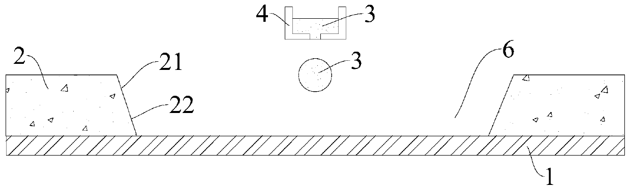
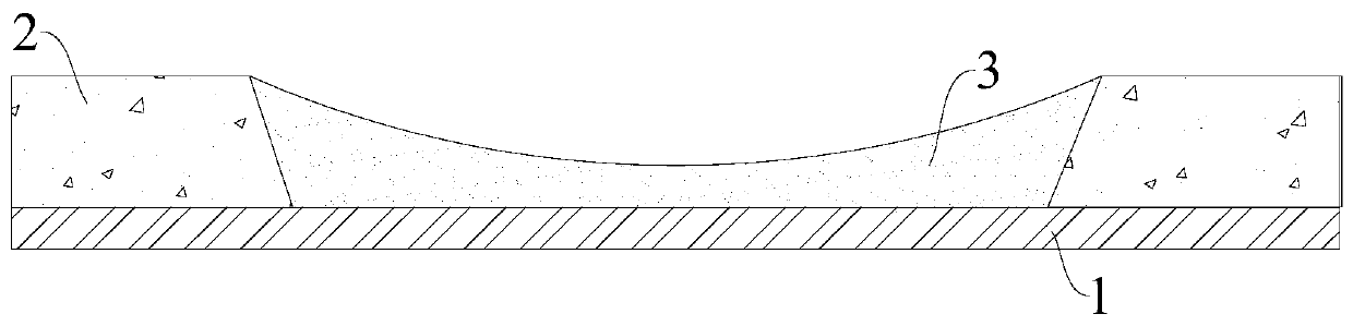
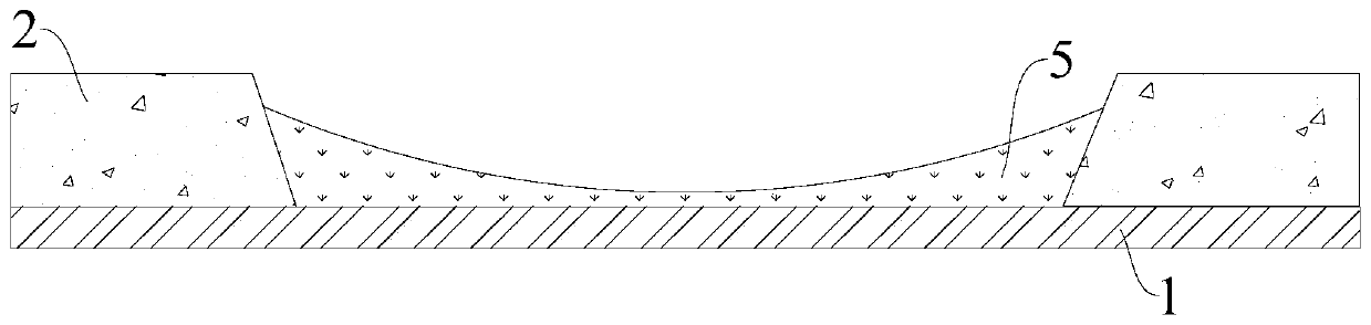
[0031] In one aspect of the invention, the invention provides a display backplane. According to an embodiment of the present invention, refer to figure 2 , the display backplane 10 includes a substrate 100, a light emitting element and a pixel defining layer, the light emitting element includes a cathode 301, an anode 302 and a light emitting layer 303, the pixel defining layer defines a plurality of ope...


PUM


Abstract

The invention provides a display backboard, a manufacturing method thereof and a display device. The display backboard comprises a substrate, a light emitting component and a pixel definition layer, the light emitting component comprises a cathode, an anode and a light emitting layer, the pixel definition layer defines multiple openings, the light emitting layer is arranged in the openings and covers a preset area, towards the side surfaces of the openings, of the pixel definition layer, and different positions in the preset area are basically consistent in hydrophilicity. The light emitting layer in the display backboard is not bent after manufacture, and the thickness of the light emitting layer is highly uniform, so that the light emitting uniformity of the display backboard is high, and the light emitting layer is avoided from overflowing out of the openings in the manufacturing process; and thus, the display backboard is avoided from electric leakage or brightening in the circumference of a pixel unit in the using process, and the display effect of the display backboard is good.

Description

technical field [0001] The present invention relates to the field of display technology, in particular, to a display backplane, a manufacturing method thereof, and a display device. Background technique [0002] At present, the organic light-emitting diode (OLED) display backplane is one of the hot spots in the field of display technology, and its aperture ratio can reach 100% in theory, which is conducive to the integration of devices and integrated circuits. That is to say, in the future, large-scale, High-definition display backplanes need to focus on active-driven organic light-emitting devices (AM-OLED). In the display backplane that actively drives organic light-emitting devices, the fabrication of the light-emitting layer mainly includes inkjet printing and the like. However, on the one hand, inkjet printing is used to make the light-emitting layer, and the resulting light-emitting layer is always prone to bending, resulting in poor uniformity of the thickness of the...

Claims


Application Information

Patent Timeline
Patent Type & Authority Applications(China)
IPC IPC(8): H01L27/32H01L51/52H01L51/56
CPCH10K59/122H10K59/12H10K50/824H10K59/1201H10K71/00H10K71/135H10K2102/351
Inventor 王国英宋振
Owner BOE TECH GRP CO LTD
Why Eureka
Try Eureka