

Display substrate, manufacturing method of display substrate and display device
A display substrate and substrate substrate technology, applied in nonlinear optics, instruments, optics, etc., can solve problems affecting the effective contact area of insulating film layers, high wiring density in the display wiring area, and affecting the reliability of display devices, etc. Achieve the effects of improving reliability, avoiding film layer shedding, and increasing binding force
- Summary
- Abstract
- Description
- Claims
- Application Information
AI Technical Summary
Problems solved by technology
Method used
Image



Examples
Embodiment Construction
[0037] In order to make the technical problems, technical solutions and advantages to be solved by the embodiments of the present invention clearer, the following will describe in detail with reference to the drawings and specific embodiments.
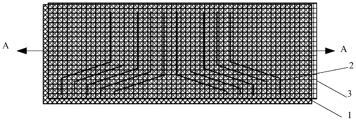
[0038] The wiring density in the wiring area of the display is relatively high, which affects the effective contact area between the insulating film layers on the upper and lower sides of the wiring line, and the phenomenon of film layer peeling is prone to occur, such as figure 1 and figure 2 As shown, in the display substrate of the related art, the source-drain metal wiring 2 is arranged on the interlayer insulating layer 1, and the side of the source-drain metal wiring 2 away from the interlayer insulating layer 1 is provided with a planar layer 3. Since the wiring The wiring density of source and drain metal wiring 2 in the area is relatively high, resulting in a small effective contact area between the interlayer insulating la...
PUM
 Abstract
Description
Claims
Application Information