

Display panel and manufacturing method thereof
A display panel and manufacturing method technology, applied in semiconductor/solid-state device manufacturing, semiconductor devices, electrical components, etc., can solve the problems of poor full-screen packaging effect, etc., and achieve the effect of improving display effect and packaging reliability
- Summary
- Abstract
- Description
- Claims
- Application Information
AI Technical Summary
Problems solved by technology
Method used
Image

Examples
Embodiment Construction
[0029] In order to make the purpose, technical solutions and advantages of the present invention clearer, the technical solutions of the present invention will be clearly and completely described through implementation with reference to the accompanying drawings in the embodiments of the present invention. Obviously, the described embodiments are the embodiment of the present invention. Some, but not all, embodiments. Based on the embodiments of the present invention, all other embodiments obtained by persons of ordinary skill in the art without making creative efforts belong to the protection scope of the present invention.
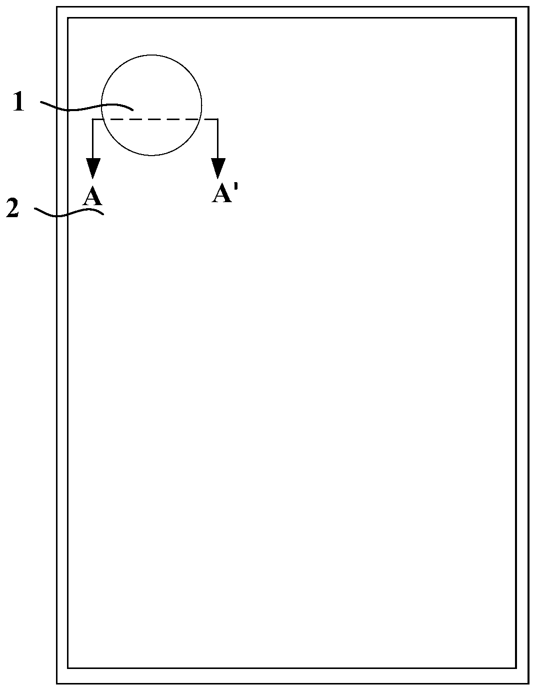
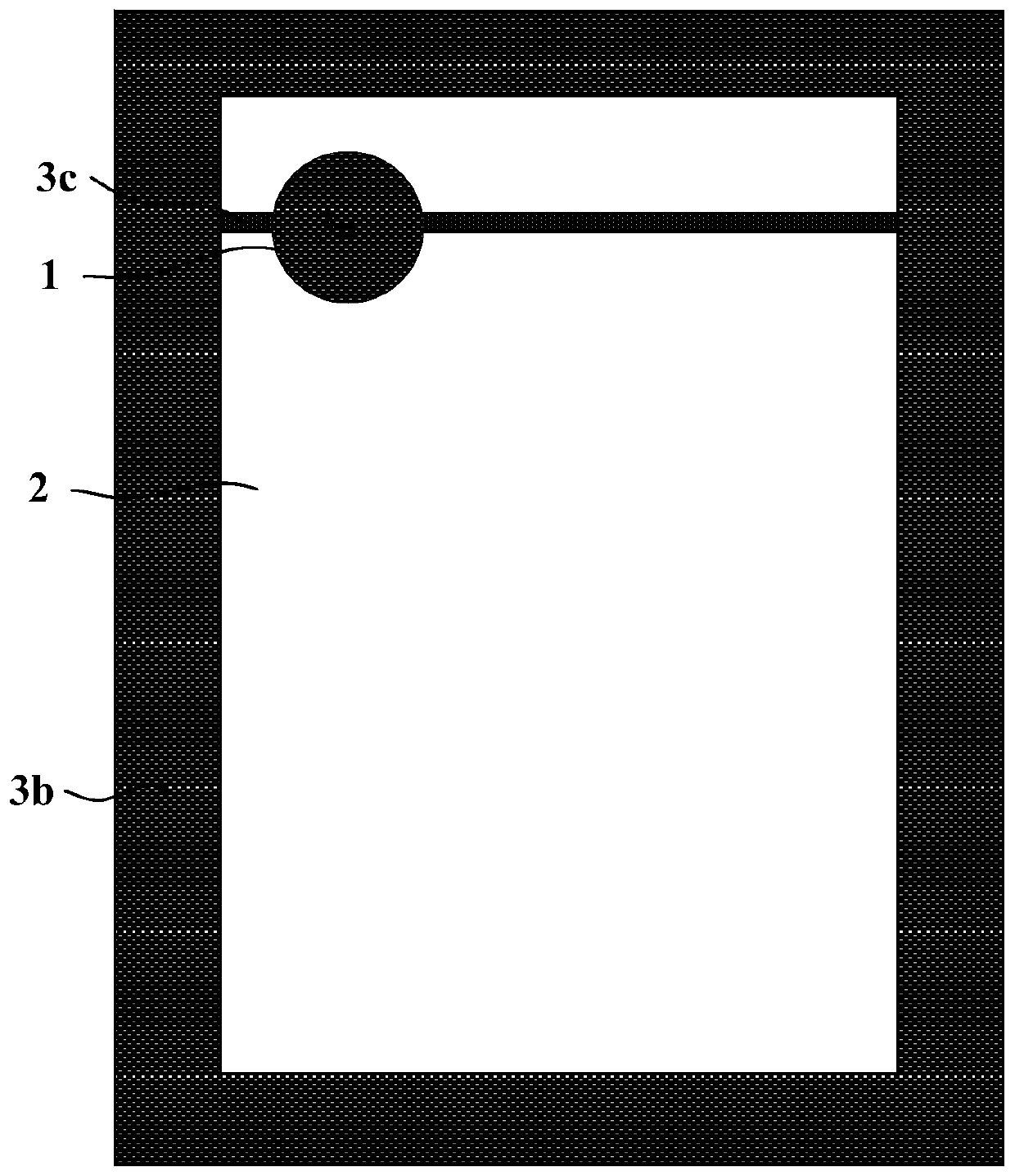
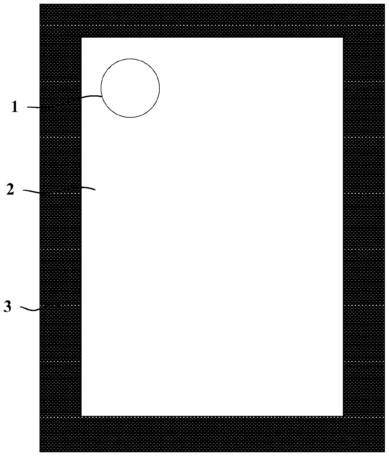
[0030] refer to figure 1 Shown is a schematic diagram of an existing full-screen display panel. The full-screen display panel is provided with a circular hole area 1, and the surrounding of the circular hole area 1 is a display area 2, and the circular hole area 1 is used to place photosensitive functional components, so as to increase the screen-to-bod...
PUM
 Abstract
Description
Claims
Application Information