


Quick Research
Generate reliable direction feasibility study reports for your R&D in just a few steps.

Technical Q&A
Discover and master advanced knowledge NOW. Basics, ideas, possibilities, all at once.

Find Solutions
As an expert in R&D theories, this can generate solutions to your technical problems instantly.

Evaluate Feasibility
Analyze your overall solution with one click, know your potential R&D risks in advance.

Monitor Landscape
Get weekly tech updates, stay abreast of the latest tech innovations and key insights.
A Parallel Analog Circuit Optimization Method Based on Genetic Algorithm and Machine Learning
A machine learning and genetic algorithm technology, applied in the field of parallel analog circuit optimization, can solve the problems of SPICE simulation time-consuming, large time cost, etc., to save time, ensure optimization accuracy, and improve optimization efficiency.
- Summary
- Abstract
- Description
- Claims
- Application Information
AI Technical Summary
Problems solved by technology
Method used
Image

Examples
Embodiment 1
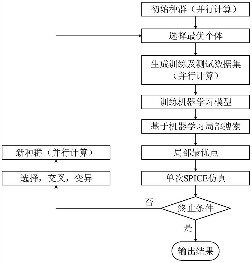
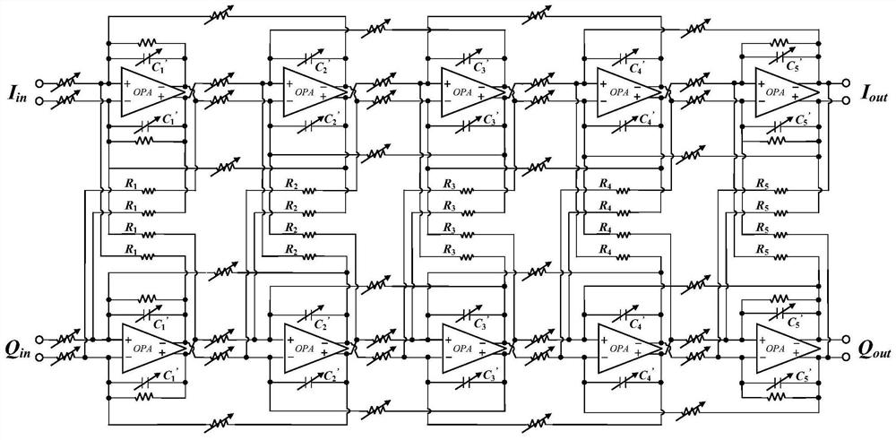
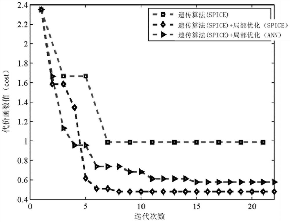
[0047] A parallel analog circuit optimization method based on genetic algorithm and machine learning, the circuit is figure 2 The fifth-order complex filter circuit shown is composed of a first low-pass filter, a second low-pass filter, and a coupling unit. Both the first low-pass filter and the second low-pass filter are 5th-order effective Source RC low-pass filter, the coupling connection unit includes 5 sets of coupling resistors. Table 1 lists the design goals of this fifth-order complex filter.
[0048] Table 1
[0049]
[0050] That is to say, the optimization goal of this embodiment is to make the passband ripple as small as possible under the premise of ensuring a center frequency of 12.24 MHz and a bandwidth of 9 MHz (deviation not exceeding 5%). For this optimization goal, five sets of coupling resistors R 1 , R 2 , R 3 , R 4 , R 5 The resistance value of is used as the circuit design variable to be optimized. The specific implementation steps are as fol...
Embodiment 2
[0083] A parallel analog circuit optimization method based on genetic algorithm and machine learning, the circuit is Figure 4 The second-order differential operational amplifier circuit shown is a fully differential second-order operational amplifier circuit for high gain and high linearity. Among them, the compensation network includes a Miller compensation capacitor and a zeroing resistor for improving phase margin.
[0084] Table 4 lists the optimization indicators of the op amp.
[0085] Table 4
[0086]
[0087] That is to say, the optimization goal of this embodiment is to increase the open-loop gain and bandwidth as much as possible on the premise of satisfying the unity gain bandwidth and phase margin. According to the symmetry requirement, the transistor M 2 , M 4 , M 6 , M 8 respectively with M 1 , M 3 , M 5 , M 7 same, that is, their widths have the following relationship: W 1 =W 2 ,W 3 =W 4 ,W 5 =W 6 ,W 7 =W 8 . In addition, the compensation ...
PUM
 Abstract
Description
Claims
Application Information
 - R&D Engineer
- R&D Manager
- IP Professional
- Industry Leading Data Capabilities
- Powerful AI technology
- Patent DNA Extraction
Browse by: Latest US Patents, China's latest patents, Technical Efficacy Thesaurus, Application Domain, Technology Topic, Popular Technical Reports.
© 2024 PatSnap. All rights reserved.Legal|Privacy policy|Modern Slavery Act Transparency Statement|Sitemap|About US| Contact US: help@patsnap.com