Display panel and display device

A display panel and display device technology, applied in the direction of semiconductor devices, electrical components, circuits, etc., can solve the problems of affecting the drive TFT gate potential, crosstalk, etc., to improve the display effect, reduce the impact, and reduce the parasitic capacitance caused by The effect of crosstalk effects

Active Publication Date: 2019-10-01
KUNSHAN GO VISIONOX OPTO ELECTRONICS CO LTD
View PDF6 Cites 5 Cited by
  • Summary
  • Abstract
  • Description
  • Claims
  • Application Information

AI Technical Summary

Problems solved by technology

Due to the parasitic capacitance between the signal line and the gate of the driving TFT in the OLED panel, the voltag

Method used


Image

  • Display panel and display device
  • Display panel and display device
  • Display panel and display device

Examples


Embodiment Construction

[0022] In order to make the purpose, technical solutions and advantages of the present invention clearer, the technical solutions in the embodiments of the present invention will be clearly and completely described below in conjunction with the embodiments of the present invention. Obviously, the described embodiments are part of the implementation of the present invention. example, not all examples. Based on the embodiments of the present invention, all other embodiments obtained by persons of ordinary skill in the art without making creative efforts belong to the protection scope of the present invention. In the case of no conflict, the following embodiments and features in the embodiments can be combined with each other.

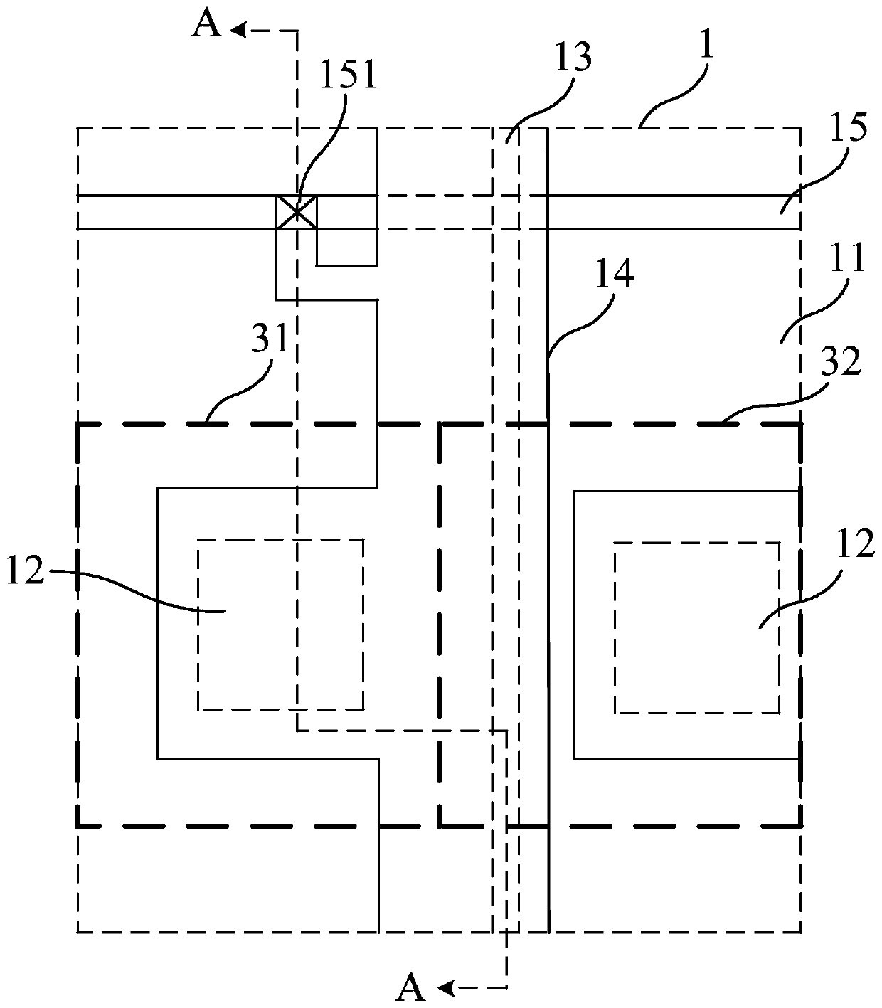
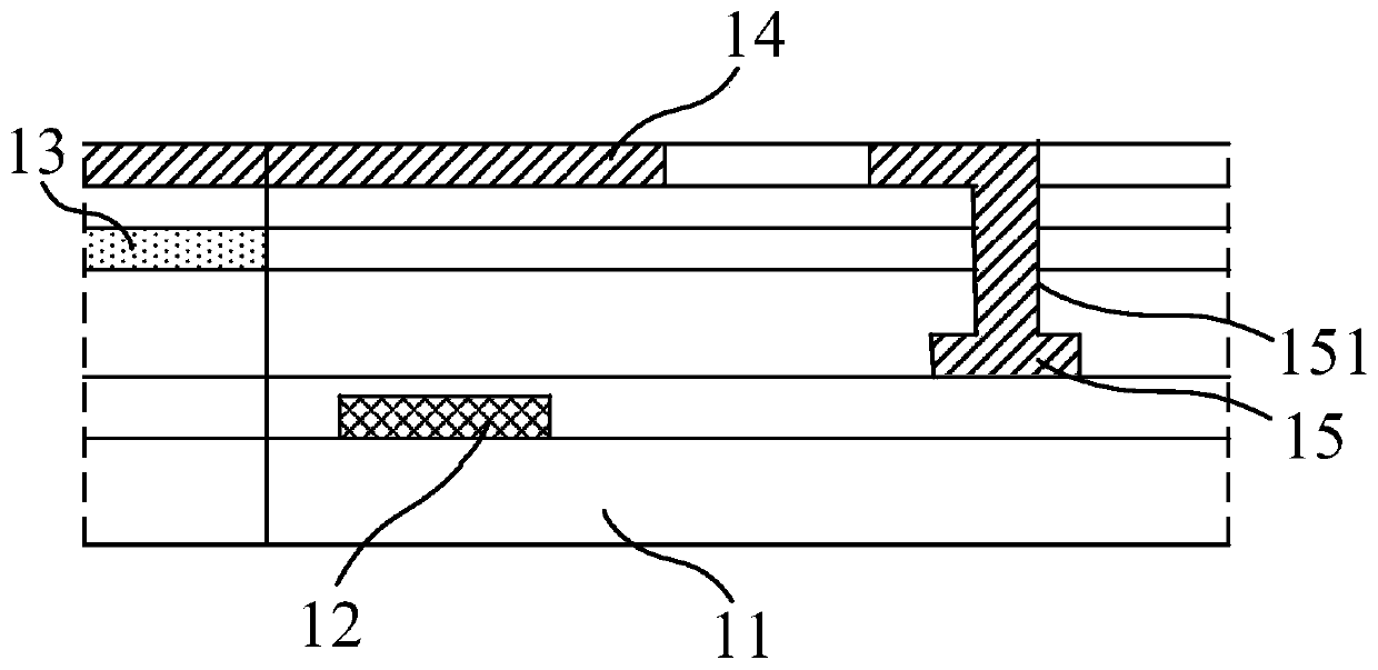
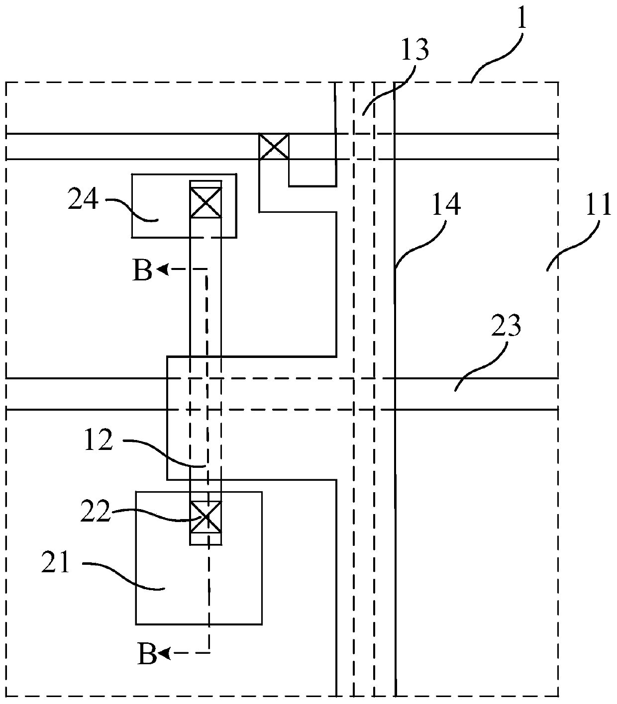
[0023] In order to solve the technical problem in the prior art that the crosstalk caused by the parasitic capacitance between the first metal trace and the second metal trace is relatively serious, an embodiment of the present invention provides a displa...


PUM


Abstract

The present invention relates to the technical field of display panels and discloses a display panel and a display device. The display panel includes a lower liner layer, a first metal trace unit, a second metal trace unit, and a third metal trace unit. The first metal trace unit is on the lower liner layer. The second metal trace unit is on the lower liner layer. The third metal trace unit is located above the first metal trace unit and the second metal trace unit and is not in contact with the first metal trace unit and the second metal trace unit, and the third metal trace unit is connectedto a fixed potential. The orthographic projections of the first metal trace unit and the second metal trace unit on the lower liner layer respectively overlap at least partially with the orthographicprojection of the third metal trace unit on the lower linear layer such that the first metal trace unit and the second metal trace unit respectively form a coupling capacitor with the third metal trace unit. In the above manner, the influence of crosstalk caused by the parasitic capacitance between the first metal trace unit and the second metal trace unit can be reduced.

Description

technical field [0001] The present invention relates to the technical field of display panels, in particular to a display panel and a display device. Background technique [0002] Currently, active matrix organic light emitting diode (Active Matrix Organic Light Emitting Display, AMOLED) displays have broad market applications. The pixels in the OLED panel are driven to emit light by the current generated by a driving thin film transistor (Driving Thin Film Transistor, DTFT) in a saturated state. Since there is a parasitic capacitance between the signal line and the gate of the driving TFT in the OLED panel, the voltage change on the signal line will affect the potential of the gate of the driving TFT, causing the problem of crosstalk. Contents of the invention [0003] In view of this, the technical problem mainly solved by the present invention is to provide a display panel and a display device capable of reducing the influence of crosstalk caused by the parasitic capac...

Claims


Application Information

Patent Timeline
IPC IPC(8): H01L27/32H01L51/52
CPCH10K59/12H10K59/131H10K50/86
Inventor 田苗苗马志丽张九占韩珍珍
Owner KUNSHAN GO VISIONOX OPTO ELECTRONICS CO LTD
Why Eureka
Try Eureka