Misplug prevention power supply, misplug prevention load and pluggable power supply misplug prevention system
A technology of anti-wrong insertion and power socket, which is applied in the field of communication, can solve the problems of increased cost, non-universal power interface shell, and inability to realize anti-wrong insertion, so as to avoid conflicts
- Summary
- Abstract
- Description
- Claims
- Application Information
AI Technical Summary
Problems solved by technology
Method used
Image
Examples
Embodiment 1
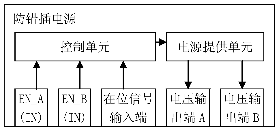
[0045] Assuming that there are two power sockets on the anti-wrong insertion load in Embodiment 1 of the present invention, which are respectively power socket one and power socket two, the anti-wrong insertion load requires two kinds of voltages, which are 12V and 54V respectively, and its power input terminals are respectively It is 12V (IN) and 54V (IN), and there is a mixed insertion situation at present. For example, a double 12V output anti-misplug power supply 1 has been inserted, that is, its power output terminals are 12V (OUT) and 12V (OUT), and then prepare Insert a 12V and 54V mixed output anti-misplug power supply 2, that is, its power output terminals are 12V (OUT) and 54V (OUT), and its system block diagram is shown in Figure 5 , wherein, the bit signal output terminal is internally connected to the secondary ground GND, the first power enable signal corresponds to a low level (“0” level), and matches the 12V voltage, and the second power enable signal correspon...
Embodiment 2
[0048] Assume that there are two power sockets on the anti-wrong insertion load in Embodiment 2 of the present invention, which are respectively power socket one and power socket two. IN) and 12V (IN), there is a mixed insertion situation at present, for example, a double 12V output anti-misplug power supply 1 has been inserted, that is, its power output terminals are 12V (OUT) and 12V (OUT), and then a 12V (OUT) is ready to be inserted The anti-misplug power supply 2 with mixed output of 54V, that is, the output terminals of the power supply are 12V(OUT) and 54V(OUT). For the system block diagram, see Figure 6 , wherein, the bit signal output terminal is internally connected to the secondary ground GND, the first power enable signal corresponds to a low level (“0” level), and matches the 12V voltage, and the second power enable signal corresponds to a high level (“0” level) 1” level), and match the 54V voltage.
[0049] At this time, because the first power enable signal in...
PUM
 Abstract
Description
Claims
Application Information
 - R&D Engineer
- R&D Manager
- IP Professional
- Industry Leading Data Capabilities
- Powerful AI technology
- Patent DNA Extraction
Browse by: Latest US Patents, China's latest patents, Technical Efficacy Thesaurus, Application Domain, Technology Topic, Popular Technical Reports.
© 2024 PatSnap. All rights reserved.Legal|Privacy policy|Modern Slavery Act Transparency Statement|Sitemap|About US| Contact US: help@patsnap.com


