Infrared touch display device
An infrared touch and display device technology, applied in optics, instruments, electrical digital data processing, etc., can solve the problem of rainbow pattern affecting visual effects, etc., and achieve the effect of improving rainbow pattern phenomenon and improving visual effect.
- Summary
- Abstract
- Description
- Claims
- Application Information
AI Technical Summary
Problems solved by technology
Method used
Image
Examples
Embodiment 1
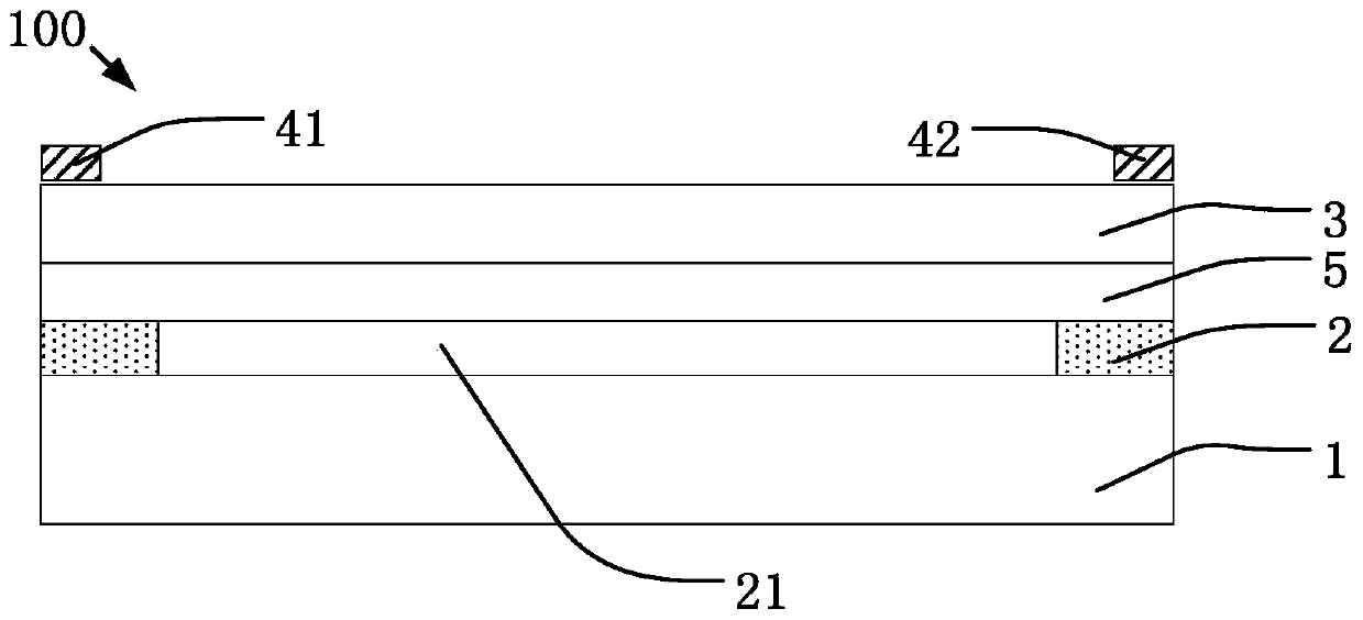
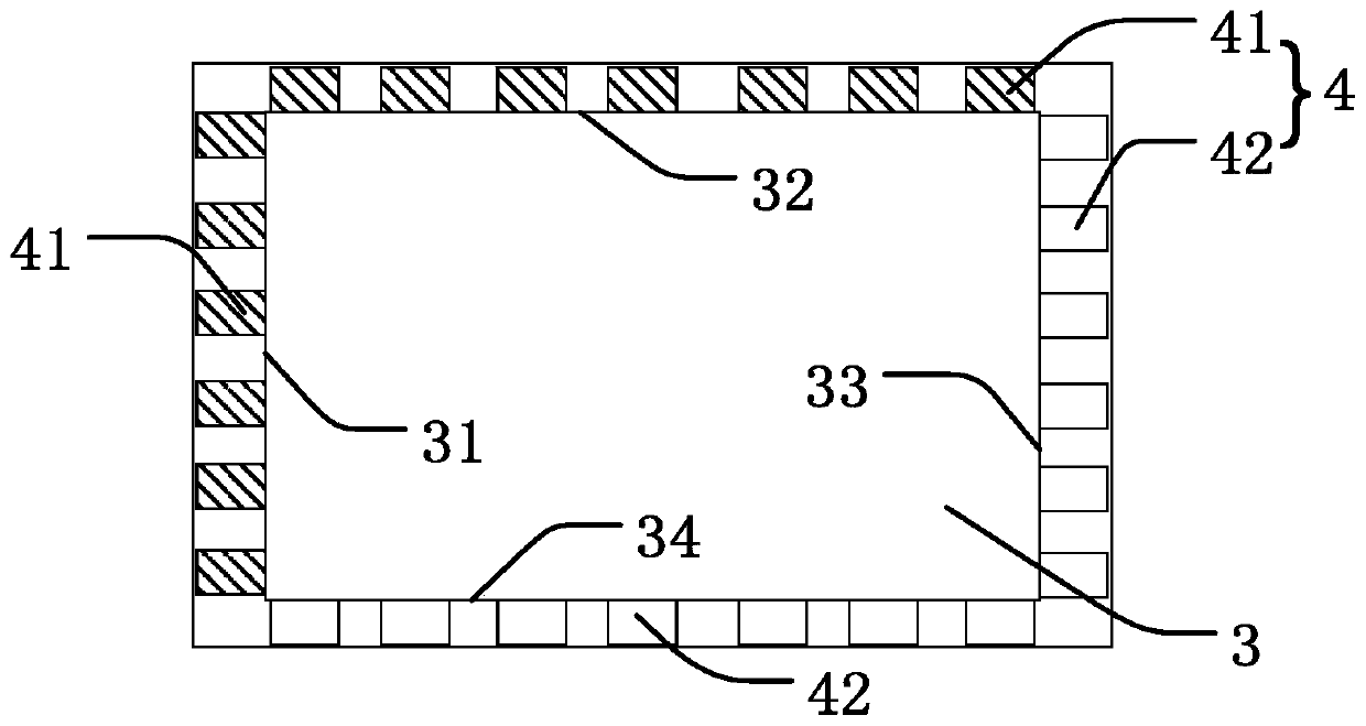
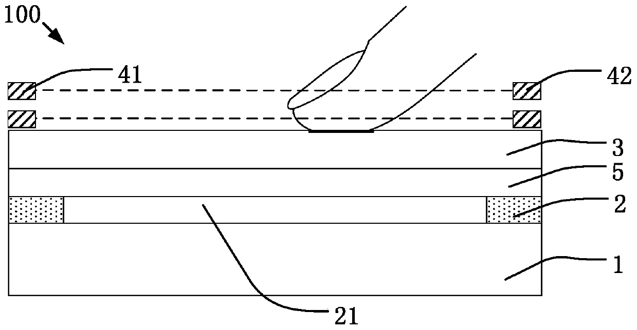
[0032] Such as figure 1 As shown, this embodiment provides an infrared touch display device 100 , which includes a display panel 1 , an optical adhesive layer 2 , a cover plate 3 , an infrared touch panel 4 and a microstructure layer 5 stacked from bottom to top.
[0033] The display panel 1 is a liquid crystal display panel, an organic light-emitting diode display panel, an active matrix organic light-emitting diode display panel, or a polymer light-emitting diode display panel.
[0034] The optical adhesive layer 2 is annularly arranged on the periphery of the upper surface of the display panel 1; the optical adhesive layer 2 surrounds to form a vacuum chamber 21; specifically, the optical adhesive layer 2 is annularly arranged on the The periphery of the upper surface of the display panel 1 ; the area surrounded by the optical adhesive layer 2 forms a vacuum chamber 21 ; in this embodiment, the optical adhesive layer 2 is preferably a rectangular ring, and the center of the...
Embodiment 2
[0046] Such as Figure 5 As shown, the second embodiment includes all the technical features of the first embodiment, the difference is that the microstructure layer 5 in the second embodiment is arranged on the display panel 1 facing the optical adhesive layer 2 The surface on one side, instead of the microstructure layer 5 in the first embodiment, is disposed on the surface of the cover plate 3 facing the optical adhesive layer 2 .
[0047] In this embodiment, the anti-glare film 51 is formed by atomizing the surface of the display panel 1 facing the optical adhesive layer 2 . The atomization treatment includes forming the anti-glare film 51 by corroding the surface of the film layer, and the microstructure layer 5 can effectively improve reflection and visual interference.
[0048] Such as Figure 4 , Figure 5 As shown, the microstructure layer 5 includes the antiglare film 51 and the base layer 52 ; the antiglare film 51 is disposed on the base layer 52 . The existenc...
Embodiment 3
[0050] Such as Figure 6a , Figure 6b As shown, in order to further enhance the display effect, the third embodiment includes all the technical features of the first embodiment and the second embodiment, the difference is that the third embodiment is further provided with a second microstructure layer 5, which is arranged between the cover plate 3 and the infrared touch panel 4.
[0051] Such as Figure 6a , Figure 6b Shown are two structural schematic diagrams in the third embodiment, Figure 6a and figure 1 The difference is that in figure 1 A second layer of microstructure layer 5 is added to the surface of the cover plate 3 facing the side of the optical adhesive layer 2; Figure 6b and Figure 5 The difference is that in Figure 5 A second layer of microstructure layer 5 is added on the surface of the display panel 1 facing the side of the optical adhesive layer 2 on the basis of . By disposing the second microstructure layer 5 above the cover 3 and disposing t...
PUM
 Abstract
Description
Claims
Application Information


