PCB laser drilling precision testing device and method

A technology of laser drilling and precision testing, which is applied in the direction of measuring devices, testing of mechanical components, testing of machine/structural components, etc., and can solve problems such as high cost

Pending Publication Date: 2019-11-15
广州广合科技股份有限公司
View PDF0 Cites 2 Cited by
  • Summary
  • Abstract
  • Description
  • Claims
  • Application Information

AI Technical Summary

Problems solved by technology

The cost is expensive, and the current cos

Method used


Image

  • PCB laser drilling precision testing device and method
  • PCB laser drilling precision testing device and method

Examples


Embodiment Construction

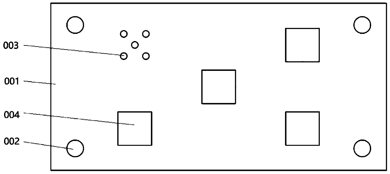
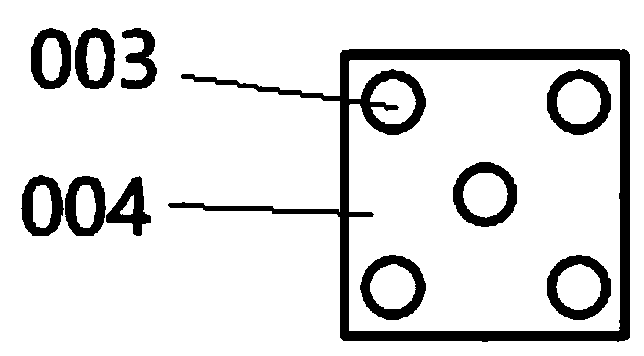
[0025] Such as Figure 1-2 As shown in , a PCB laser drilling precision test device provided by an embodiment of the present invention is characterized in that: it includes a test board 001, and a plurality of positioning holes 002 and a plurality of test holes 003 are opened on the test board 001. Several sheets of rectangular kraft paper 004 are attached to the surface of the test board 001, and each sheet of kraft paper 004 covers the openings of five test holes 003, and the five test holes 003 are respectively located at the center and four corners of the rectangular kraft paper 004.

[0026] Further, the kraft paper 004 is attached to the surface of the test board 001 by crumpled tape.

[0027] Further, the test hole 003 is a through hole with a diameter of 0.4 mm.

[0028] A testing method is also provided: a PCB laser drilling accuracy testing method, comprising the following steps:

[0029] S1, board making, select the PCB board as the test board 001, and drill a num...


PUM

PropertyMeasurementUnit
Diameteraaaaaaaaaa
Diameteraaaaaaaaaa
Thicknessaaaaaaaaaa

Abstract

The present invention relates to a PCB laser drilling precision testing device, which comprises a test board. The test board is provided with a plurality of positioning holes and a plurality of test holes. The surface of the test board is attached with several sheets of rectangular kraft paper, each of which covers apertures of five test holes; and the five test holes are respectively located at the center and four corners of the rectangular kraft paper. Compared with high test cost of a professional testing device, the device can realize the precision test of a laser drilling machine at the cost of several sheets of kraft paper.

Description

technical field [0001] The invention relates to the field of PCB laser drilling detection, in particular to a PCB laser drilling accuracy testing device and method. Background technique [0002] PCB is a printed circuit board. In the process of gradual development of electronic technology, the miniaturization and miniaturization of electronic equipment is constantly improving. One of the technical problems is the miniaturization of printed circuit boards. The smaller the size of the PCB board, the higher the requirements for the size and accuracy of drilling holes on the PCB board. Relying on the traditional mechanical drilling method has become more and more stretched. First of all, mechanical drilling requires high strength of the drill pin, so the diameter of the drill pin is limited and cannot be too thin. Secondly, mechanical drilling has requirements for the distance between holes. If the distance between holes is too small, the force generated by the rotation of the...

Claims


Application Information

Patent Timeline
IPC IPC(8): G01B21/00G01M13/00
CPCG01B21/00G01M13/00
Inventor 钟根带巩杰李政福
Owner 广州广合科技股份有限公司
Why Eureka
Try Eureka