Method for improving sensitivity of strain sensor by optical assistance
A stress sensor, light-assisted technology, applied in the field of stress sensors and sensors, can solve problems such as low sensitivity
- Summary
- Abstract
- Description
- Claims
- Application Information
AI Technical Summary
Problems solved by technology
Method used
Image

Examples
Embodiment 1
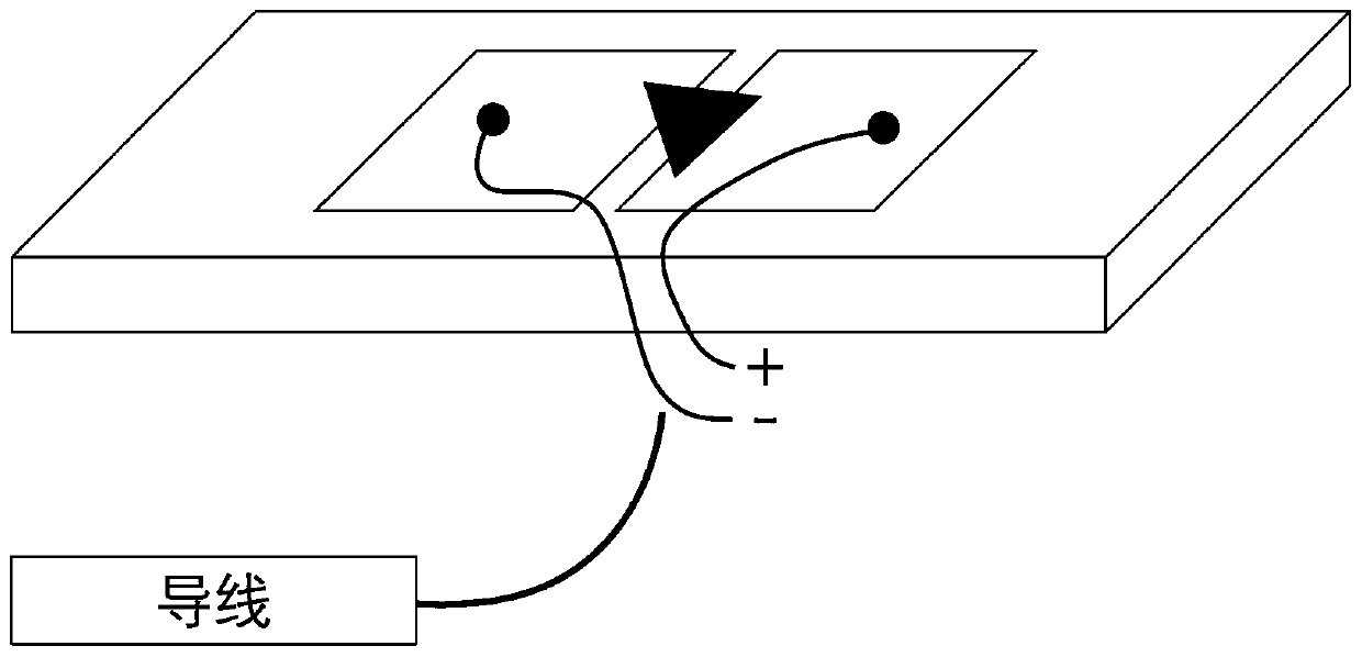
[0030] A method for light-assisted enhancement of the sensitivity of stress sensors such as Figure 5 , 6 As shown, the light-assisted method is used: the stress sensor based on the two-dimensional material receives light while the electrical property changes under the influence of the stress; the light is used as an auxiliary function to inject additional carriers into the two-dimensional material, so that the electrical property changes The amplitude is increased, so as to achieve the purpose of improving the sensitivity of the stress sensor.
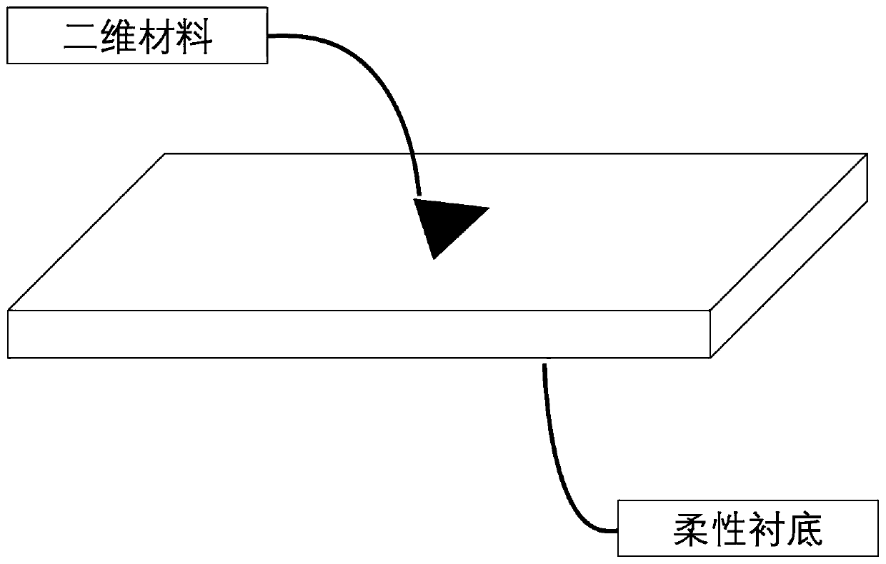
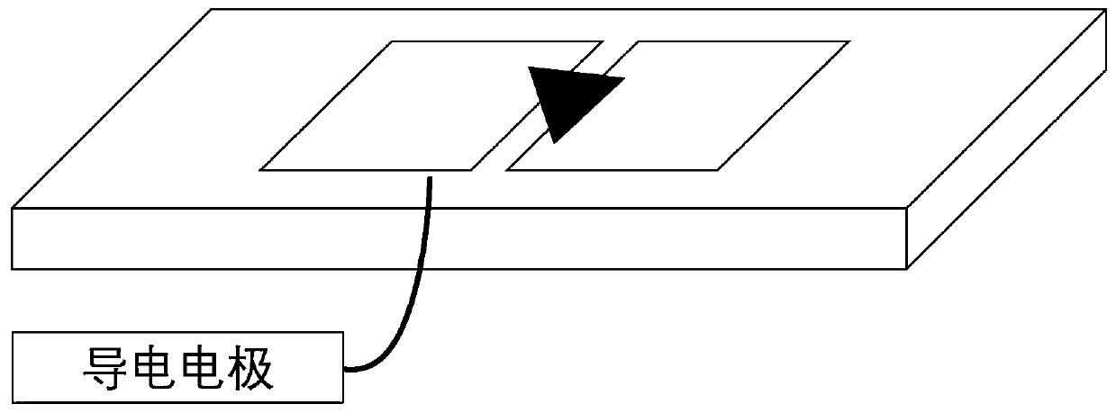
[0031] The high-sensitivity stress sensor prepared by the above method includes: a two-dimensional material, a flexible substrate, a conductive electrode, a wire and a light source; the two-dimensional material is placed on the flexible substrate, and the conductive electrode is placed on the two-dimensional material and the flexible between the substrates; illuminate the two-dimensional material part with a light source; connect wir...
PUM
 Abstract
Description
Claims
Application Information
 - R&D
- Intellectual Property
- Life Sciences
- Materials
- Tech Scout
- Unparalleled Data Quality
- Higher Quality Content
- 60% Fewer Hallucinations
Browse by: Latest US Patents, China's latest patents, Technical Efficacy Thesaurus, Application Domain, Technology Topic, Popular Technical Reports.
© 2025 PatSnap. All rights reserved.Legal|Privacy policy|Modern Slavery Act Transparency Statement|Sitemap|About US| Contact US: help@patsnap.com