NVRAM array device with enhanced write and erase

a technology of array devices and random access memory, applied in the direction of semiconductor devices, electrical devices, transistors, etc., can solve the problems of only storing data in random access memory, write and erase cycle times, and potential damage to the storage medium

Inactive Publication Date: 2002-09-03
GLOBALFOUNDRIES INC
View PDF12 Cites 22 Cited by
  • Summary
  • Abstract
  • Description
  • Claims
  • Application Information

AI Technical Summary

Benefits of technology

It is another object of the invention to provide increased write and erase tunnelling current in a non-volatile semiconductor memory device without compromising cell size, operating margins, reliability or manufacturing yield.

Problems solved by technology

In general, random access memories can only store data when power is applied thereto.
However, magnetic storage devices rely on relative movement between the storage medium and a reading device in order to write and erase data on the medium and the mechanical arrangement for doing so is subject to wear, damage or malfunctions and is a source of potential damage to the storage medium, as well.
However, since tunnelling currents are very small, the write and erase cycle times have remained relatively intractable, consistent with reliability and small cell size.
Reduced thickness of floating gate insulation can reduce the needed amount of stored charge but increases susceptibility to damage by tunnelling currents and increasing leakage with use as well as possibly compromising manufacturing yield.
For a given thickness of floating gate insulator, reduced stored charge corresponds to reduced operating margins and increased possibility of read errors.
Likewise, increase of tunnelling current by operation at increased write and erase voltages also increases the likelihood of insulator damage.
Such cycle times certainly do not compare favorably with the bandwidth of current magnetic media.
No significant reduction in write and erase cycle times has been achieved that does not compromise cell size, operating margins, reliability and / or manufacturing yield.

Method used


Image

  • NVRAM array device with enhanced write and erase
  • NVRAM array device with enhanced write and erase
  • NVRAM array device with enhanced write and erase

Examples


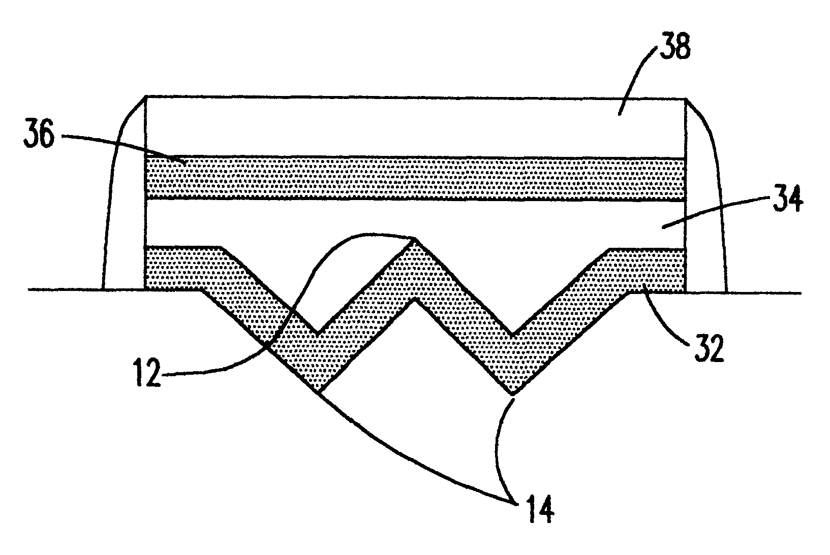
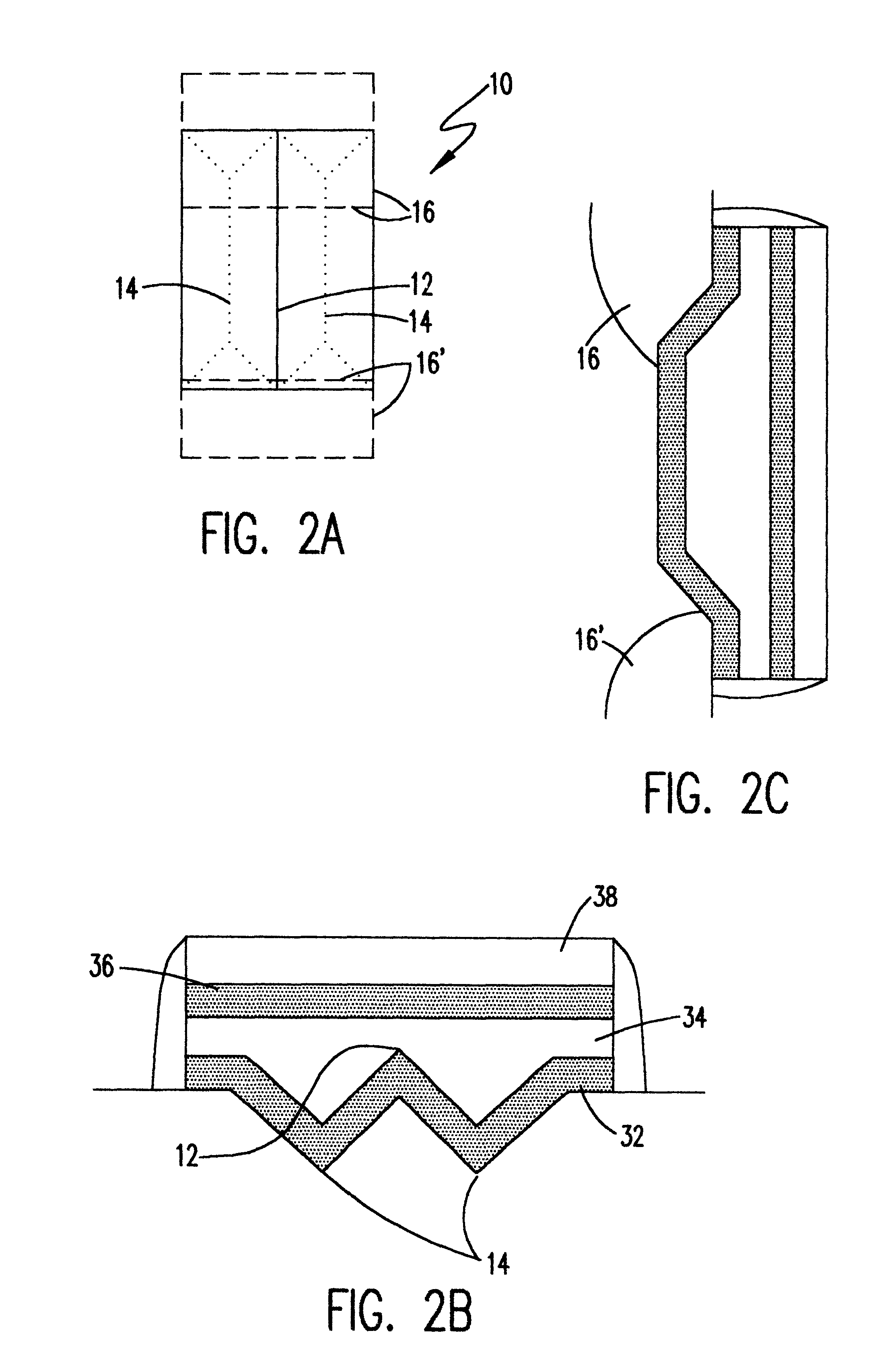
Embodiment Construction

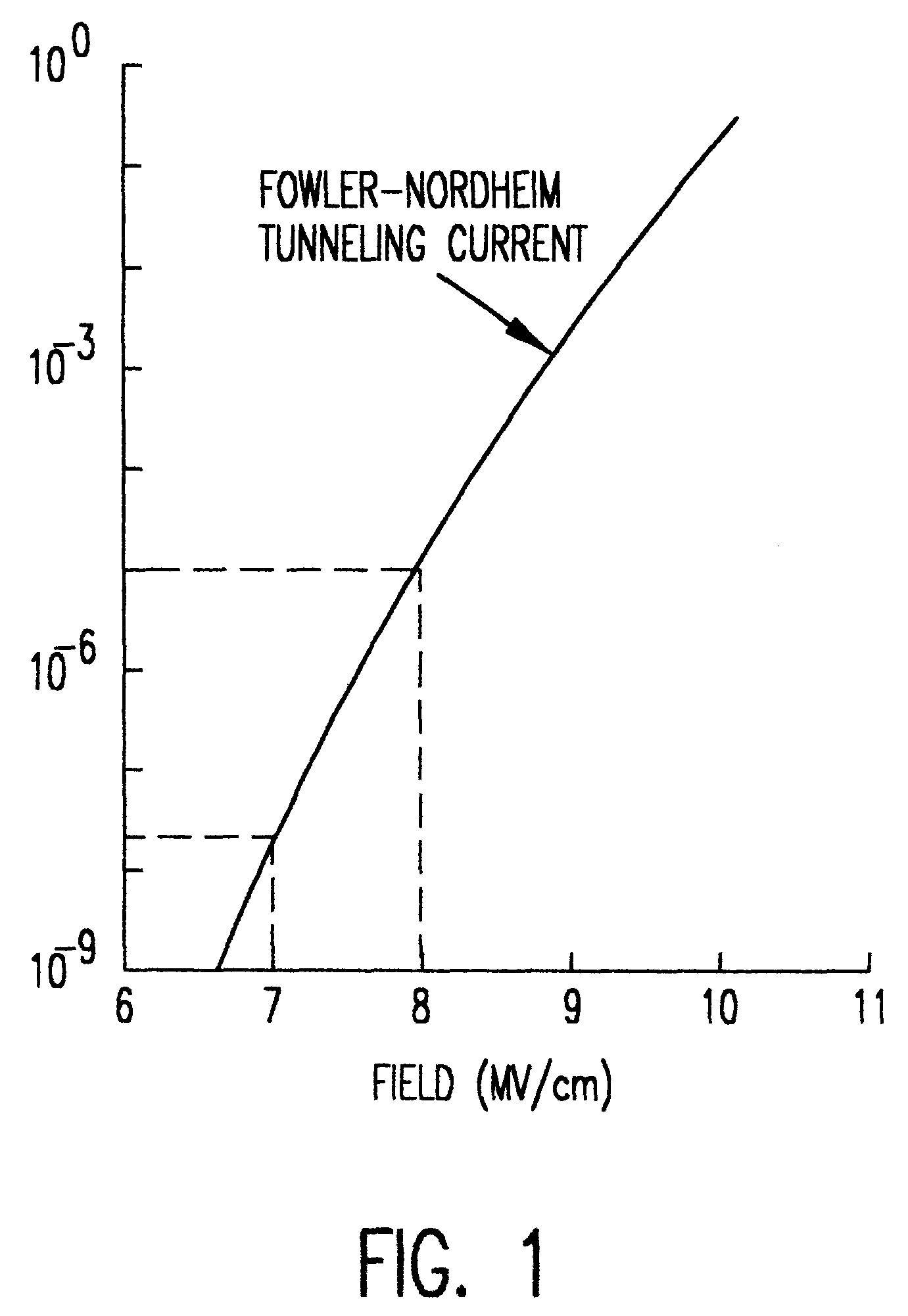
Referring now to the drawings, and more particularly to FIG. 1, there is shown a graph of Fowler-Nordheim current density as a function of electric field. This graph is published in "Flash Memory Cells--An Overview" by Paolo Pavan et al.; Proceedings of the IEEE Vol. 85, No. 8: August 1997: pp. 1248-1271. It is apparent from FIG. 1 that current density increases sharply and almost exponentially with increases in electrical field.

However, as alluded to above, increasing operating voltage sufficiently to obtain a significant increase in current density is not feasible since other important qualities of a non-volatile memory cell storing such tunnelling current would be severely compromised. Additionally, higher voltages requires higher voltage power supplies, more robust power conditioning circuitry and high power requirements while many NVRAM applications, such as smart cards, necessarily require low power operation and supporting circuits of very small size. Accordingly, a basic pri...


PUM


Abstract

Increased write and erase tunnelling currents are developed by enhancement of an electric field near a floating gate with a shaped edge structure overlapping a source / drain diffusion and developing increased floating gate area with angled regions joined by edges in order to reduce write and erase cycle times. The edge structure is formed by selective and preferential etching in accordance with the crystal structure of a monocrystalline semiconductor substrate. The sharpness of the edges and concentration of the electric field may be enhanced by consumption and stress effects of oxidation of the substrate to form a floating gate insulator.

Description

1. Field of the InventionThe present invention generally relates to non-volatile random access memory (NVRAM) arrays and, more particularly, to arrays of memory cells formed as a field effect transistor having a floating gate on which charge can be placed by tunnelling effects.2. Description of the Prior ArtDigital signal processing arrangements such as microprocessors use many different types of memory and storage structures for different purposes. The type of memory used will often be determined by the needed speed of access, the length of time data will be stored and the operational circumstances during storage of data. For example, a read-only memory (ROM) is used for data which is necessary for operation of the processor and never changed while a random access memory (RAM) of either a static or dynamic type is used for the working memory of the processor and access speed may be enhanced by the use of one or more levels of caching. In general, random access memories can only sto...

Claims


Application Information

Patent Timeline
Patent Type & Authority Patents(United States)
IPC IPC(8): H01L21/02H01L27/115H01L21/28H01L29/40H01L29/423H01L21/8247H01L29/788
CPCH01L21/28273H01L27/115H01L29/42336H01L29/40114H10B69/00H01L29/788H10B99/00
Inventor LAM, CHUNG H.WILLIAMS, RICHARD Q.
Owner GLOBALFOUNDRIES INC
Why Eureka
Try Eureka