Preparation method of semiconductor substrate layer and preparation method of solar cell

A semiconductor and substrate layer technology, applied in the field of solar cells, can solve the problem of high reflectivity of silicon substrates

Active Publication Date: 2022-07-26
ANHUI HUASUN ENERGY CO LTD
View PDF6 Cites 0 Cited by
  • Summary
  • Abstract
  • Description
  • Claims
  • Application Information

AI Technical Summary

Problems solved by technology

[0005] Therefore, the technical problem to be solved by the present invention is to overcome the defect of high reflectivity of the silicon substrate of the existing solar cell, and then provide a method for preparing a semiconductor substrate layer and a method for preparing a solar cell

Method used


Image

  • Preparation method of semiconductor substrate layer and preparation method of solar cell
  • Preparation method of semiconductor substrate layer and preparation method of solar cell
  • Preparation method of semiconductor substrate layer and preparation method of solar cell

Examples


Embodiment 1

[0038] This embodiment provides a method for preparing a semiconductor substrate layer, such as figure 1 shown, including the following steps:

[0039] Step S1: providing an initial semiconductor substrate layer;

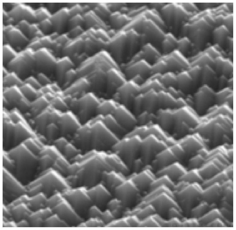
[0040] Step S2: using an alkaline solution to perform a first texturing treatment on the surface of the initial semiconductor substrate layer;

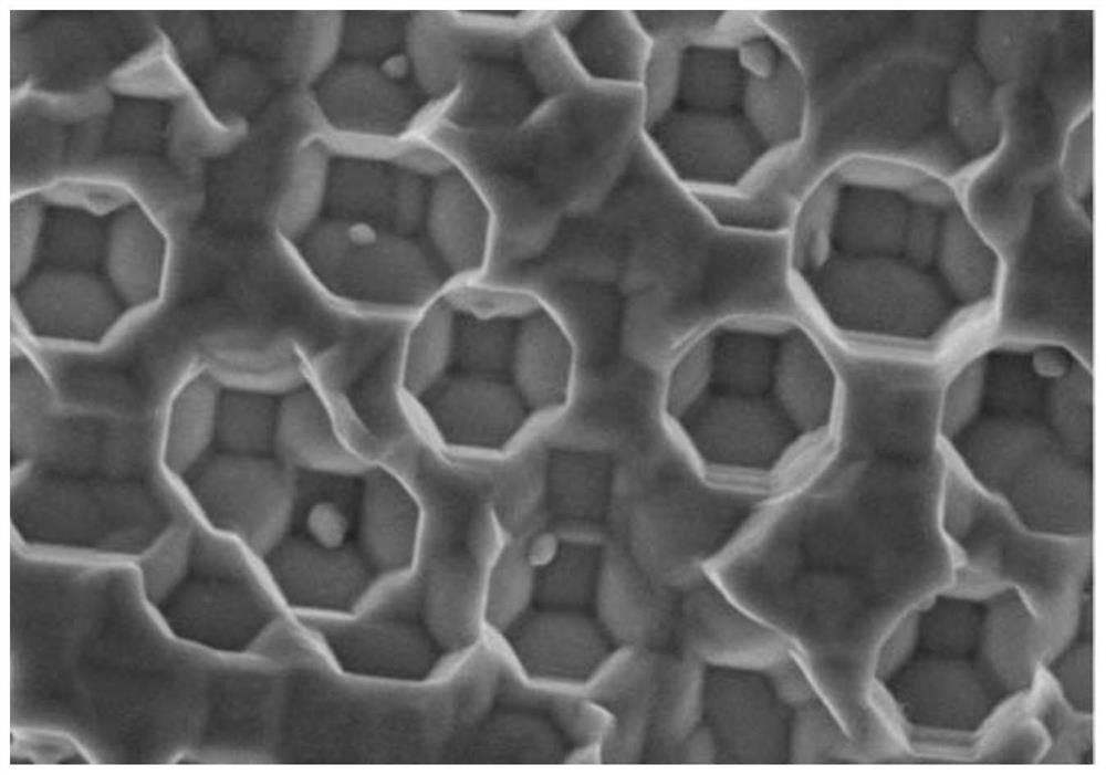
[0041] Step S3: After the first texturing treatment is performed, a second texturing treatment is performed on the surface of the initial semiconductor substrate layer by using a metal-catalyzed chemical etching process.

[0042]If a conventional method is used to form a textured surface directly on the semiconductor substrate layer by a metal-catalyzed chemical etching process, the reflectivity of the textured surface will be relatively high, which is not conducive to the entry of light into the solar cell, resulting in a decrease in the current density of the solar cell. In the present invention, the surface of the init...

Embodiment 2

[0056] This embodiment provides a method for fabricating a solar cell, including: forming a semiconductor substrate layer, where the semiconductor substrate layer is formed by using the method for fabricating a semiconductor substrate layer. A textured structure is formed on the surface of the semiconductor substrate layer, and the textured structure is in the micrometer scale and is only a very thin part of the layered structure of the solar cell. Generally, the thickness dimension of the solar cell is 10,000 times to 100,000 times the thickness dimension of the textured structure.

[0057] Optionally, it further includes: forming a first intrinsic passivation layer on one side surface of the semiconductor substrate layer; forming a second intrinsic passivation layer on the other side surface of the semiconductor substrate layer; A first doped semiconductor layer is formed on a surface of an intrinsic passivation layer away from the semiconductor substrate layer; a second dop...


PUM


Abstract

The invention relates to the technical field of solar cells, and particularly provides a preparation method of a semiconductor substrate layer and a solar cell. The preparation method of the semiconductor substrate layer comprises the following steps: providing an initial semiconductor substrate layer; carrying out first texturing treatment on the surface of the initial semiconductor substrate layer by adopting an alkaline solution; and after the first texturing treatment is carried out, carrying out second texturing treatment on the surface of the initial semiconductor substrate layer by adopting a metal catalysis chemical etching process. According to the invention, on the basis that the alkaline solution is adopted to carry out the first texturing treatment on the surface of the initial semiconductor substrate layer, the metal catalytic chemical etching process is adopted to carry out the second texturing treatment on the surface of the initial semiconductor substrate layer, so that on the basis of the pyramid of the alkaline texturing surface, the characteristic of preferential etching of metal catalytic etching is combined, and the etching efficiency is improved. And the inverted pyramid suede with lower reflectivity is prepared by adjusting process parameters.

Description

technical field [0001] The invention relates to the technical field of solar cells, in particular to a preparation method of a semiconductor substrate layer and a preparation method of a solar cell. Background technique [0002] The solar cell has developed rapidly in recent years, which is a device that directly or indirectly converts solar radiation energy into electrical energy through the photoelectric effect or the photochemical effect. Heterojunction cells are an important type of solar cells. By changing the properties of PN junctions, the photoelectric conversion efficiency of heterojunction cells can be improved. In addition, heterojunction cells have the characteristics of good temperature coefficient, double-sided power generation, low process temperature, and high photoelectric conversion efficiency, and are very competitive solar cell technologies in the market. [0003] Texturing is an important process for silicon wafers to form a good substrate, forming an e...

Claims


Application Information

Patent Timeline
Patent Type & Authority Applications(China)
IPC IPC(8): H01L31/18H01L31/0236H01L21/306C30B33/10
CPCH01L31/1804H01L31/02363H01L21/30608C30B33/10Y02P70/50
Inventor 龚道仁徐晓华周肃周锡伟梅志纲
Owner ANHUI HUASUN ENERGY CO LTD
Why Eureka
Try Eureka