Method for manufacturing a defect-controlled low-oxygen concentration silicon single crystal wafer

a technology of low-oxygen concentration and silicon single crystal, which is applied in the direction of single crystal growth, polycrystalline material growth, chemistry apparatus and processes, etc., can solve the problems of increased leak current, reduced breakdown voltage, and high cost of epitaxial wafers, and achieves low cost and good productivity.

Active Publication Date: 2017-05-16
SHIN-ETSU HANDOTAI CO LTD
View PDF16 Cites 0 Cited by
  • Summary
  • Abstract
  • Description
  • Claims
  • Application Information

AI Technical Summary

Benefits of technology

[0045]As described above, according to the present invention, the silicon single crystal wafer that is suitable for, e.g., a power device can be manufactured with good productivity at a low cost.

Problems solved by technology

If crystal defects or BMDs (Bulk Micro Defects) formed by precipitation of oxygen are present in a region where such a current flows, a problem of decrease of a breakdown voltage or increase of leak current may possibly occur.
However, since an epitaxial wafer is expensive or a degree of difficulty of manufacturing of an FZ crystal rises at the time of increasing a diameter, the respective cases have problems.

Method used


Image

  • Method for manufacturing a defect-controlled low-oxygen concentration silicon single crystal wafer
  • Method for manufacturing a defect-controlled low-oxygen concentration silicon single crystal wafer
  • Method for manufacturing a defect-controlled low-oxygen concentration silicon single crystal wafer

Examples


examples

[0088]Although the present invention will now be more specifically explained hereinafter based on examples and comparative examples, the present invention is not restricted thereto.

experiment 1

[0089]Defect characteristics of a low-oxygen crystal were first grasped.

[0090]A defect distribution in a silicon crystal having usual oxygen concentration relative to a growth rate is as schematically shown in FIG. 4(a). A vacancy dominant region is provided on a high growth rate side, and an interstitial Si dominant region is provided on a low growth rate side.

[0091]In the high rate side region, many silicon single crystal ingots having different oxygen concentration values were grown in the region where vacancies are sufficiently dominant that OSF nuclei are considered to adhere to an outer periphery when a wafer is sliced out. Wafer-shaped samples are sliced out from these silicon single crystal ingots and subjected to an FPD evaluation. As observation of FPDs, the wafer samples were subjected to surface grinding, cleaning, and mirror etching using a mixed acid, then the samples were left in an preferential etchant consisting of a hydrofluoric acid, a nitric acid, an acetic acid,...

experiment 2

[0098]Further, to see an influence given on defects that are detected as the FPDs by the oxygen concentration, an experiment of investigating a defect region while changing a growth rate was conducted.

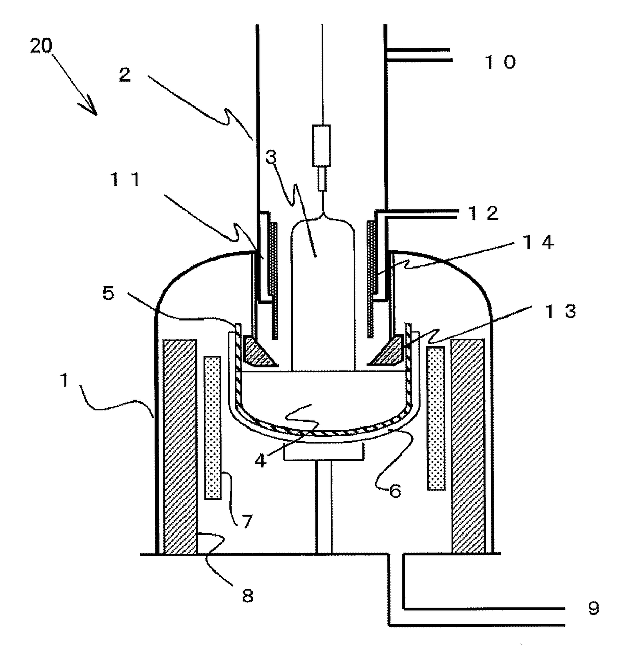
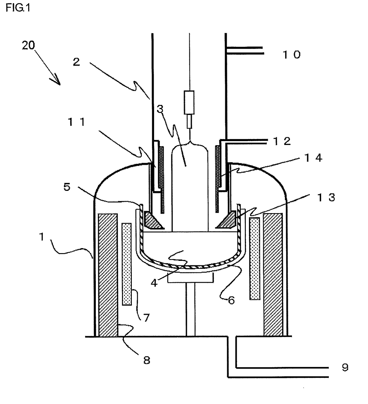
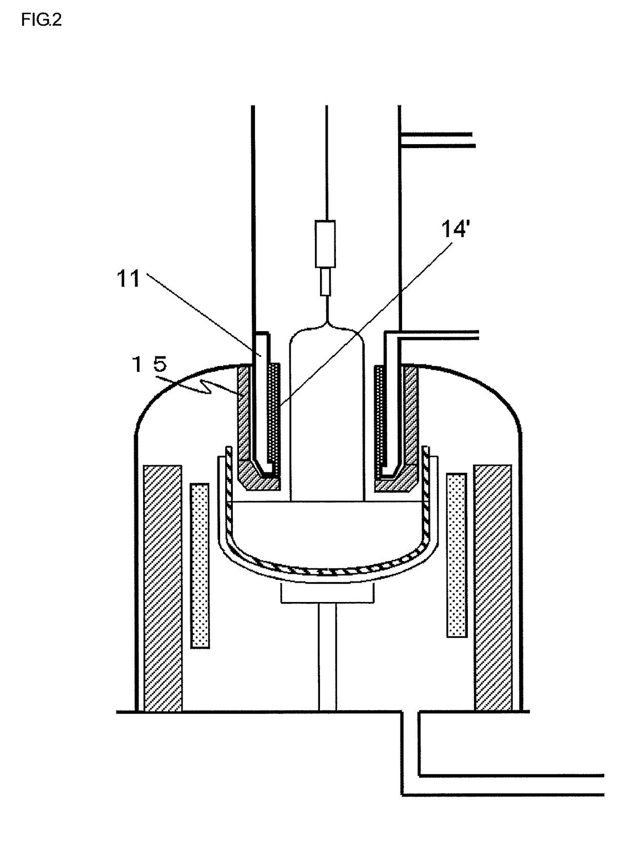
[0099]As a single crystal manufacturing apparatus and a hot zone (HZ), the apparatus shown in FIG. 1 was used. This single crystal manufacturing apparatus has a water-cooled SUS cooling cylinder that is extended from ceiling portion of a main chamber toward a surface of a raw material melt and is formed into a cylindrical shape that surrounds a silicon single crystal ingot. Furthermore, a cooling auxiliary cylinder is fitted in this cylinder. This cooling auxiliary cylinder is made of a graphite material. Moreover, slit 16 cleaving in the longitudinal direction as shown in FIG. 3 is formed in the cooling auxiliary cylinder. A lower end of the cooling auxiliary cylinder is configured to extend to a lower side of a lower end of the cooling cylinder and cool the silicon single crystal ing...


PUM

PropertyMeasurementUnit
temperatureaaaaaaaaaa
diameteraaaaaaaaaa
melting pointaaaaaaaaaa

Abstract

The present invention provides a method for manufacturing a silicon single crystal wafer, wherein, under a growth condition that V / G≧1.05×(V / G)crt is achieved where V is a growth rate in growth of the silicon single crystal ingot, G is a temperature gradient near a crystal growth interface, and (V / G)crt is a value of V / G when a dominant point defect changes from a vacancy to interstitial Si, a silicon single crystal ingot having oxygen concentration of 7×10¹⁷ atoms / cm3 (ASTM'79) or less is grown, and a silicon single crystal wafer which includes a region where the vacancy is dominant and in which FPDs are not detected by preferential etching is manufactured from the grown silicon single crystal ingot. As a result, there is provided the method that enables manufacturing a low-oxygen concentration silicon single crystal wafer that can be preferably used for a power device with good productivity at a low cost.

Description

BACKGROUND OF THE INVENTION[0001]1. Field of the Invention[0002]The present invention relates to a method for manufacturing a defect-controlled low-oxygen concentration silicon single crystal wafer used in advanced technology fields such as a memory, a CPU, or a power device in particular.[0003]2. Description of the Related Art[0004]In relation to energy saving, power devices is recently attracting attention. These devices are different from other devices such as memory, a large current flows through a wafer. A region in which a current flows is not restricted to an extremely shallow surface layer as different from the prior art, it may be a range having a thickness of tens or hundreds μm from the surface layer, or the current may flow in a thickness direction depending on a device.[0005]If crystal defects or BMDs (Bulk Micro Defects) formed by precipitation of oxygen are present in a region where such a current flows, a problem of decrease of a breakdown voltage or increase of leak...

Claims


Application Information

Patent Timeline
Patent Type & Authority Patents(United States)
IPC IPC(8): C30B15/20C30B29/06
CPCC30B15/203C30B29/06
Inventor HOSHI, RYOJIKAMADA, HIROYUKISUGAWARA, KOSEI
Owner SHIN-ETSU HANDOTAI CO LTD
Why Eureka
Try Eureka