Method of making a semiconductor device by balancing shallow trench isolation stress and optical proximity effects

a technology of isolation stress and optical proximity, applied in the direction of individual semiconductor device testing, semiconductor/solid-state device testing/measurement, instruments, etc., can solve the problems of not being able to address device operational or electrical characteristics that vary, feature distortion, and not being able to achieve stress relief at the edg

Active Publication Date: 2006-05-18
BELL SEMICON LLC
View PDF1 Cites 26 Cited by
  • Summary
  • Abstract
  • Description
  • Claims
  • Application Information

AI Technical Summary

Benefits of technology

[0008] To address the above-discussed deficiencies of the prior art, the present invention provides a method for manufacturing a semiconductor device, comprising: determining an isolation structure stress effect of a first semiconductor device, determining an optical proximity effect of a second semiconductor device, selecting a modeling design parameter such that the isolation structure stress effect is offset against the optical proximity effect on a fabrication model, and using the selected design parameter to construct a third semiconductor device.
[0009] In another embodiment, the present invention provides a system for producing a semiconductor device model for use in fabricating an integrated circuit. This particular embodiment includes an isolation structure stress effect subsystem for providing isolation structure stress effect data of a first semiconductor device, an optical proximity effect subsystem for providing optical proximity effect data of a second semiconductor device, a design layout subsystem that uses the isolation structure stress effect data and the optical proximity effect data to derive a model design layout such that the isolation structure stress effect is offset against the optical proximity effect, and a production design subsystem that uses the model design layout to model a production semiconductor device that includes an integrated circuit layout.
[0010] In another embodiment, the present invention provides a semiconductor device that comprises device features defined by a mask wherein the features are formed thru values selected by balancing shallow trench isolation stress effect with optical processing correction effect.

Problems solved by technology

This, in turn, allows diffraction that can cause feature distortion.
However, while this often satisfactorily addresses critical dimension concerns, it fails to address device operational or electrical characteristics that vary from those predicted by the design layout modeling processes and that are influenced by spacing between multi-strip gate structures, both active and dummy structures.
The reason for this is that when the edges of the STI come closer together, there is not enough distance between the edges for stress relief itself.
For example, STI stress effect has been found to cause drive current degradations in MOSFETS and has also been found to cause defect and device leakage.
As mentioned above, for very deep, sub-micron processes, it, is difficult to print onto silicon the exact desired device shape due to the exposure limitations inherent in the lithographic processes.
Patterning is affected because features have become so small that the light photography does not replicate the features well, particularly at device sizes of 130 nm, 90 nm, 65 nm and below.
These variations occur because the features have become so small that with optical processing, the wavelength is not small enough to print everything accurately due to reflections and diffractions from the mask.
As a result, the desired image does not get printed accurately.

Method used


Image

  • Method of making a semiconductor device by balancing shallow trench isolation stress and optical proximity effects
  • Method of making a semiconductor device by balancing shallow trench isolation stress and optical proximity effects
  • Method of making a semiconductor device by balancing shallow trench isolation stress and optical proximity effects

Examples


Embodiment Construction

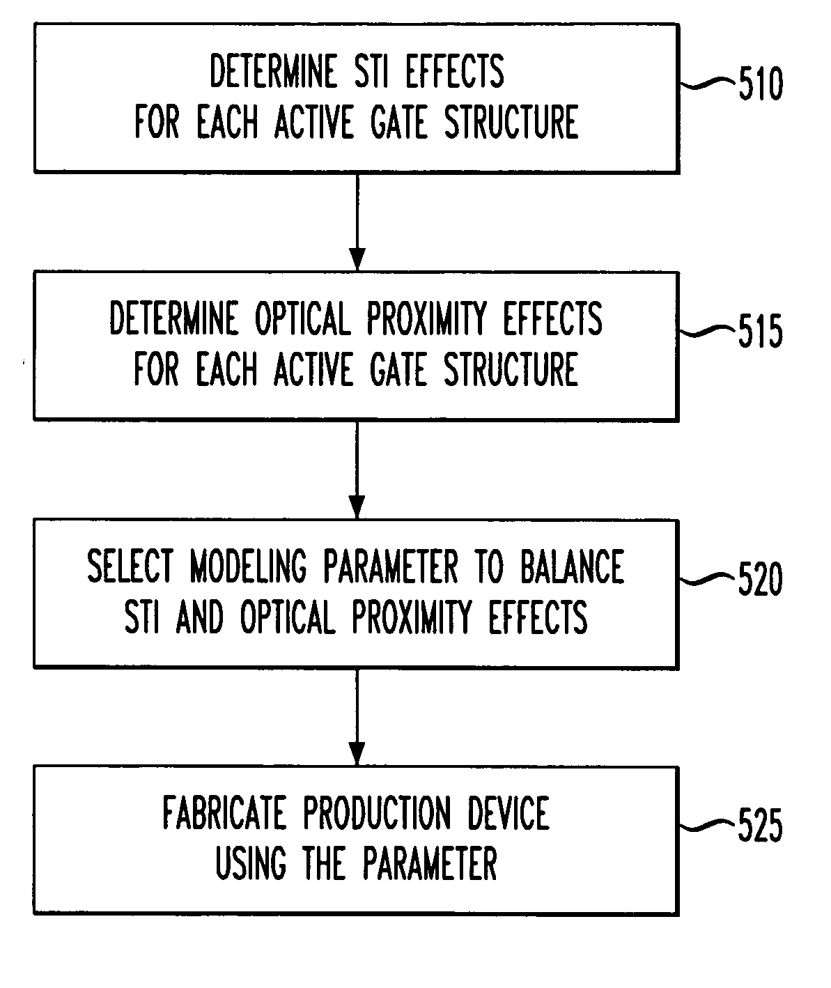
[0021] The present invention uniquely recognizes the benefits associated with using the shallow trench isolation stress effect (hereinafter referred to as the STI stress effect) and the optical proximity effect and their relationship to various electrical properties of a transistor to provide a more accurate correlation between a design model of an integrated circuit and a production device of that integrated circuit. Presently, it has been recognized that the STI effect and the optical proximity effect can each be correlated to an electrical characteristic of a transistor, such as on current (Ion), off current (Ioff), or threshold voltage (VT). It has further been presently recognized that the STI effect and optical proximity effect influence the electrical properties of the transistor devices. The present invention recognizes that these two effects, along with their relationship to those electrical properties, can be used in the transistor design layout such that the STI and the o...


PUM


Abstract

The present invention provides a method for manufacturing a semiconductor device, comprising: determining an isolation structure stress effect of a first semiconductor device, determining an optical proximity effect of a second semiconductor device, selecting a modeling design parameter such that the isolation structure stress effect is offset against the optical proximity effect on a fabrication model, and using the selected design parameter to construct a third semiconductor device.

Description

TECHNICAL FIELD OF THE INVENTION [0001] The present invention is directed, in general, to semiconductor fabrication processes and, more specifically, to a method and system that balances isolation structure stress effects against optical proximity effects to insure that modeling performance is more accurately reflected in actual production devices. BACKGROUND OF THE INVENTION [0002] The fabrication of a semiconductor device involves hundreds of steps, each of which must be executed as accurately as possible to achieve a high-yield, functioning device. The beginning steps of fabrication begin with an electrical schematic of the integrated circuit, which is converted to a design layout that is used to ultimately construct a lithographic mask. As device sizes have moved well into the submicron range and component density has significantly increased, the accuracy of the lithographic processes has diminished inasmuch as many of the feature sizes have become smaller than the wavelength th...

Claims


Application Information

Patent Timeline
Patent Type & Authority Applications(United States)
IPC IPC(8): G06F17/50
CPCG06F17/5068H01L21/76224H01L27/0207G06F30/39
Inventor CHLIPALA, JAMES D.MOINIAN, SHAHRIAR
Owner BELL SEMICON LLC
Why Eureka
Try Eureka