Logic BRAM mapping method and system

A mapping method and logic technology, applied in the field of logical BRAM mapping technology, can solve problems such as resource waste and filling failure, and achieve the effects of reducing waste, making up for resource waste, and optimizing the traversal filling process

Active Publication Date: 2019-11-22
SHANGHAI ANLOGIC INFOTECH CO LTD
View PDF10 Cites 0 Cited by
  • Summary
  • Abstract
  • Description
  • Claims
  • Application Information

AI Technical Summary

Problems solved by technology

[0003] However, there may be multiple types of ERAM resources in the FPGA. When filling only a single type of ERAM, the filling may fail because the number of any single type of ERAM remaining in the FPGA is not enough to complete the filling of the logical BRAM mapping area. ; Moreover, even if there is sufficient amount of any single type of ERAM remaining in the FPGA, the result of filling only a single type of ERAM will often cause more waste of resources

Method used


Image

  • Logic BRAM mapping method and system
  • Logic BRAM mapping method and system
  • Logic BRAM mapping method and system

Examples


Embodiment Construction

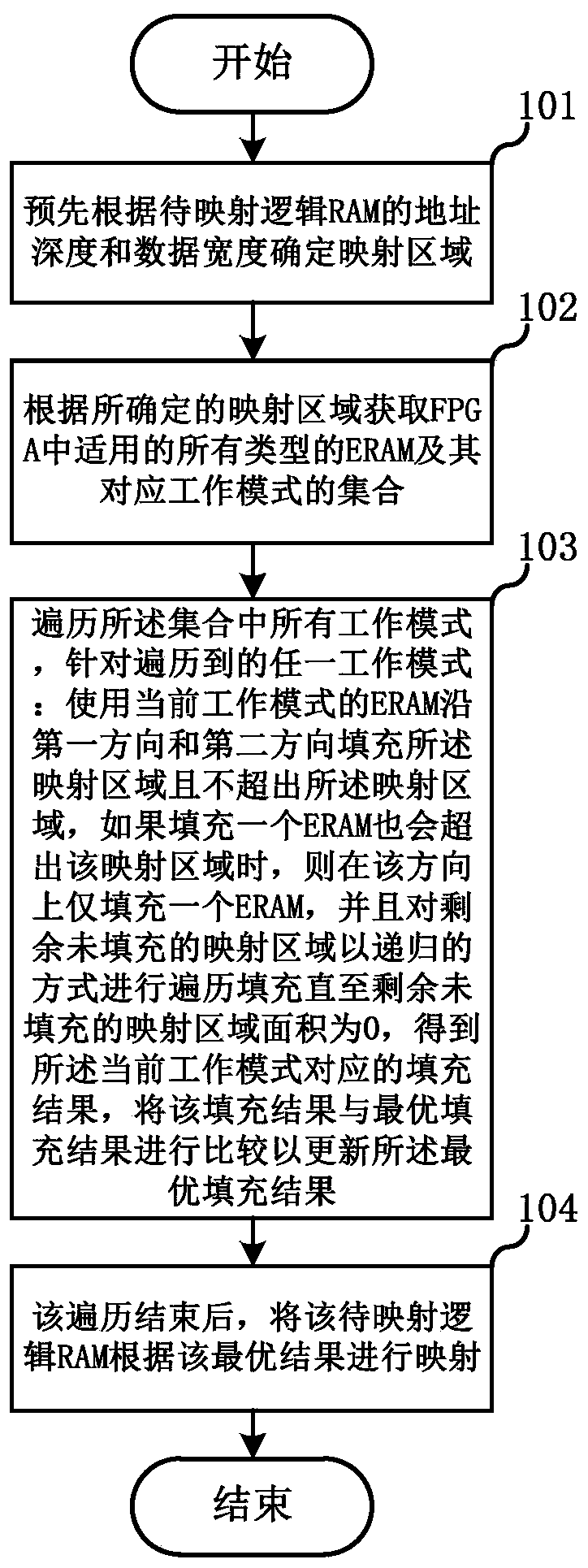
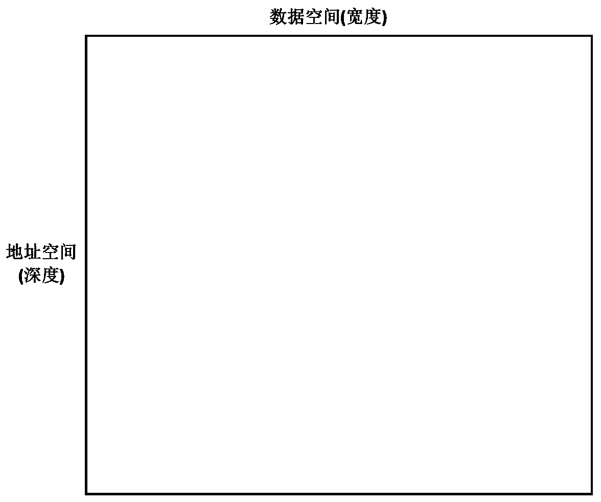
[0050] In the following description, many technical details are proposed in order to enable readers to better understand the application. However, those skilled in the art can understand that the technical solutions claimed in this application can be realized even without these technical details and various changes and modifications based on the following implementation modes.

[0051] Explanation of some concepts:

[0052] FPGA: Field Programmable Gate Array, Field Programmable Logic Array. It appeared as a semi-custom circuit in the field of application-specific integrated circuits, which not only solved the shortcomings of full-custom circuits, but also overcome the shortcomings of the limited number of gates of the original programmable logic device.

[0053] ERAM: Embeded Random Access Memory, embedded random access memory. A hardware storage resource customized in FPGA has a fixed size and can be randomly accessed according to address and clock.

[0054] BRAM: Block R...


PUM


Abstract

The invention relates to the field of integrated circuits, and discloses a logic BRAM mapping method and system. The method comprises the following steps: determining a mapping area according to a logic BRAM to be mapped; according to the mapping area, obtaining sets of all types of applicable ERAMs and corresponding working modes thereof; traversing operating modes in a set, aiming at any traversed working mode, using the ERAM in the current working mode to fill in the first direction and the second direction and not exceeding the mapping area; if filling of one ERAM is also exceeded, only filling one ERAM in the direction, carrying out traversal filling on the remaining unfilled mapping areas in a recursive mode until the areas of the remaining unfilled mapping areas are zero, obtaininga filling result, and updating the optimal filling result according to the filling result; and after traversal is finished, mapping the logic BRAM to be mapped according to the optimal result. According to the embodiment of the invention, the method can enable various types of ERAM resources to be fully and reasonably utilized while meeting the filling demands of the mapping region of the logic BRAM, and reduces the resource waste.

Description

technical field [0001] This application relates to the field of integrated circuits, in particular to the mapping technology of logic BRAM. Background technique [0002] In the existing FPGA logic BRAM mapping process, generally for a single type of ERAM, one or more pieces of ERAM are used to fill the mapping area size of the logic BRAM. [0003] However, there may be multiple types of ERAM resources in the FPGA. When filling only a single type of ERAM, the filling may fail because the number of any single type of ERAM remaining in the FPGA is not enough to complete the filling of the logical BRAM mapping area. ; Moreover, even if the amount of any single type of ERAM remaining in the FPGA is sufficient, the result of filling only a single type of ERAM often causes more waste of resources. Contents of the invention [0004] The purpose of the present application is to provide a logical BRAM mapping method and system thereof, which can make full and reasonable use of vari...

Claims


Application Information

Patent Timeline
IPC IPC(8): G06F12/06
CPCG06F12/0646
Inventor 余伟余建德
Owner SHANGHAI ANLOGIC INFOTECH CO LTD
Why Eureka
Try Eureka