Display substrate, preparation method thereof and display device
A technology for displaying substrates and substrates, which is applied in the direction of electrical components, electrical solid devices, circuits, etc., and can solve the problems of low resolution of transparent display devices
- Summary
- Abstract
- Description
- Claims
- Application Information
AI Technical Summary
Problems solved by technology
Method used
Image

Examples
Embodiment Construction
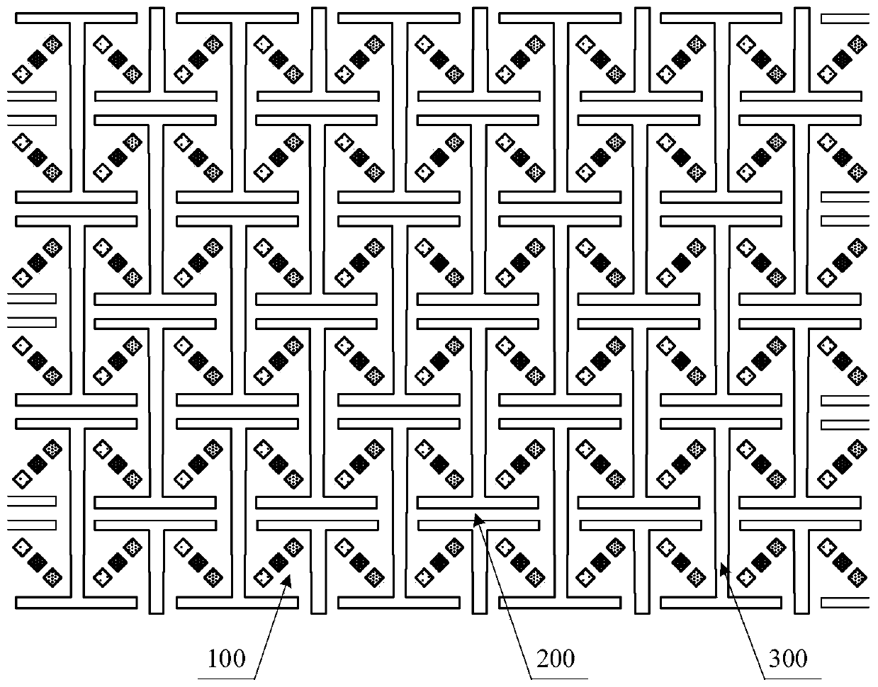
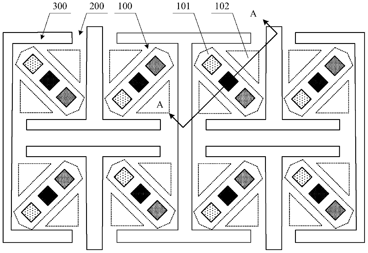
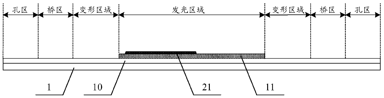
[0057] The specific implementation manners of the present invention will be further described in detail below in conjunction with the accompanying drawings and examples. The following examples are used to illustrate the present invention, but are not intended to limit the scope of the present invention. It should be noted that, in the case of no conflict, the embodiments in the present application and the features in the embodiments can be combined arbitrarily with each other.
[0058] The inventors of the present application have found through research that existing transparent display devices have problems such as low resolution, which are caused by the relatively large area of the transparent region. Generally, to achieve a better transparent display effect, the light transmittance of the display device needs to reach more than 90%. For the existing structure in which each display unit is divided into a display area and a transparent area, it is necessary to design the a...
PUM
 Abstract
Description
Claims
Application Information