Method for detecting dielectric constant of material by using scanning probe

A technology for detecting dielectric constant and materials, applied in scanning probe technology, scanning probe microscopy, measuring electrical variables, etc., can solve problems such as difficult scanning analysis, achieve simple modeling process, and realize non-destructive detection Effect

Active Publication Date: 2020-01-10
NANJING UNIV OF POSTS & TELECOMM
View PDF12 Cites 4 Cited by
  • Summary
  • Abstract
  • Description
  • Claims
  • Application Information

AI Technical Summary

Problems solved by technology

[0002] In the prior art, the dielectric constant is an important inherent property of dielectric materials. Generally speaking, the relative permittivity of metals (referred to as dielectric constant) is very large, and the better the dielectric insulation performance, the smaller the dielectric constant. An extreme case is: the dielectric constant of an ideal conductor is infinite, and the dielectric constant of a vacuum is 1; at present, the conventional means of measuring the dielectric constant is mainly an optical ellipsometer. complex refractive index, extinction coefficient, and dielectric constant; usually, the spot size of an ellipsometer requires at least tens of microns, so it is difficult to scan and analyze materials at the nanometer scale; with the development of semiconductor integrated circuits, microelectronic and optoelectronic materials The characteristic size of the device has entered the submicron or even nanometer level, and the analysis of the dielectric properties of these micro-nano electronic devices requires the introduction of new methods; on the other hand, since the atomic force microscope was invented in the late 1980s, Scanning probe microscopy has experienced vigorous development, and various extended modes—such as Kelvin mode, electrostatic force mode, conductive mode, magnetic force mode, piezoelectric force mode—have been developed and widely used in the surface analysis of micro-nano electronic materials Among them; the present invention is based on electrostatic force microscope technology, proposes a kind of new method that utilizes scanning probe to detect the permittivity of dielectric materials such as semiconductors at the nanometer scale

Method used


Image

  • Method for detecting dielectric constant of material by using scanning probe
  • Method for detecting dielectric constant of material by using scanning probe
  • Method for detecting dielectric constant of material by using scanning probe

Examples


Embodiment Construction

[0031] Embodiments of the present invention will be described in detail below in conjunction with the accompanying drawings.

[0032] A method for detecting the dielectric constant of a material using scanning probe microscopy, comprising the steps of:

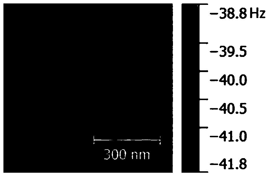
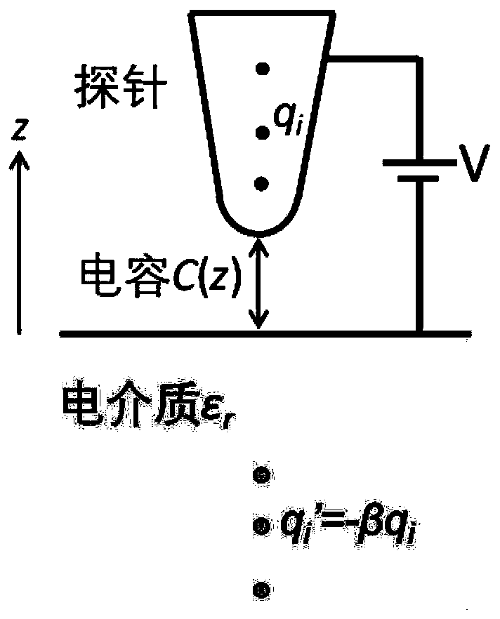
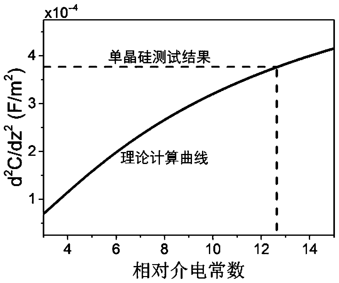
[0033] (1) Using an electrostatic force microscope: under DC bias, keep the distance z between the probe and the sample constant, detect the offset Δf of the resonance frequency of the probe, and calculate the capacitance between the probe and the sample accordingly second derivative d 2 C / dz 2 ; The second derivative d 2 C / dz 2 It can also be represented by C";

[0034] (2) Using the image charge method: construct a relationship model between the force and capacitance between the probe and the sample as the dielectric constant ε changes in the sample, and obtain the C"-ε curve;

[0035] (3), d in step (1) 2 C / dz 2 The calculated experimental value is compared with the theoretical curve of C"-ε in step (2), to obtain th...


PUM

PropertyMeasurementUnit
angleaaaaaaaaaa
lengthaaaaaaaaaa
Resonant frequencyaaaaaaaaaa

Abstract

The invention discloses a method for detecting a dielectric constant of a material by using the scanning probe microtechnique. The method comprises the following steps: firstly, obtaining an experimental value of a capacitance gradient between a probe and a sample by utilizing electric field gradient detection of an electrostatic force microscope; establishing a theoretical model of the capacitance between the probe samples along with the dielectric constant change of the samples by utilizing a mirror image charge method; and finally, comparing the experimental value with a theoretical model to deduce the dielectric constant of the sample. The method can obtain the dielectric constant information of the sample under the nanoscale, has the advantage of nondestructive detection, and is suitable for characterization of various dielectric materials such as insulators or semiconductors.

Description

technical field [0001] The invention relates to a method for detecting the dielectric constant of a material by using a scanning probe. Background technique [0002] In the prior art, the dielectric constant is an important inherent property of dielectric materials. Generally speaking, the relative permittivity of metals (referred to as dielectric constant) is very large, and the better the dielectric insulation performance, the smaller the dielectric constant. An extreme case is: the dielectric constant of an ideal conductor is infinite, and the dielectric constant of a vacuum is 1; at present, the conventional means of measuring the dielectric constant is mainly an optical ellipsometer. complex refractive index, extinction coefficient, and dielectric constant; usually, the spot size of an ellipsometer requires at least tens of microns, so it is difficult to scan and analyze materials at the nanometer scale; with the development of semiconductor integrated circuits, microel...

Claims


Application Information

Patent Timeline
Patent Type & Authority Applications(China)
IPC IPC(8): G01Q60/00G01R27/26
CPCG01Q60/00G01R27/2623
Inventor 许杰陈剑锋陈龙于天祺蔡远凌云
Owner NANJING UNIV OF POSTS & TELECOMM
Why Eureka
Try Eureka