Low-power waveguide photodetector with optical isolation between photosensitive mesa and n-contact mesa

An optical isolation and optical waveguide technology, applied in semiconductor devices, electrical components, circuits, etc., to suppress the space charge effect, increase the effective absorption length, and alleviate the mutual constraints between bandwidth and quantum efficiency.

Active Publication Date: 2021-07-13
CHONGQING UNIV OF POSTS & TELECOMM
View PDF4 Cites 0 Cited by
  • Summary
  • Abstract
  • Description
  • Claims
  • Application Information

AI Technical Summary

Problems solved by technology

[0004] In order to solve the problem of mutual restriction between the quantum efficiency and high-speed response of the semiconductor photodetector in the prior art, the present invention improves the structure of the existing waveguide photodetector; designs a monolithic optical waveguide and photodetector Integrated, low-power waveguide photodetector with broadband, high quantum efficiency, and high output power; where the photosensitive mesa is optically isolated from the N-contact mesa, and a metal film is deposited as a light reflector, and the mesa is fabricated at the end of the optical waveguide And deposit a metal thin film as a light reflector, so as to better confine the light on the photosensitive table and improve the quantum efficiency of the device, thereby alleviating the contradiction of the sharp decrease in quantum efficiency when the miniaturized active area increases the bandwidth of the device. A Solution to Simultaneously Achieve High Quantum Efficiency and Broadband

Method used


Image

  • Low-power waveguide photodetector with optical isolation between photosensitive mesa and n-contact mesa
  • Low-power waveguide photodetector with optical isolation between photosensitive mesa and n-contact mesa

Examples


Embodiment Construction

[0017] The technical solutions in the embodiments of the present invention will be described clearly and in detail below with reference to the drawings in the embodiments of the present invention. The described embodiments are only some of the embodiments of the invention.

[0018] The technical scheme of the present invention to solve the above-mentioned technical problems is: a monolithic integrated low-power waveguide photodetector structure is proposed, which solves the mutual restriction problem between the quantum efficiency and frequency response bandwidth of traditional semiconductor photodetectors, and can be widely used In optical fiber communication, satellite communication and optical signal processing and other fields.

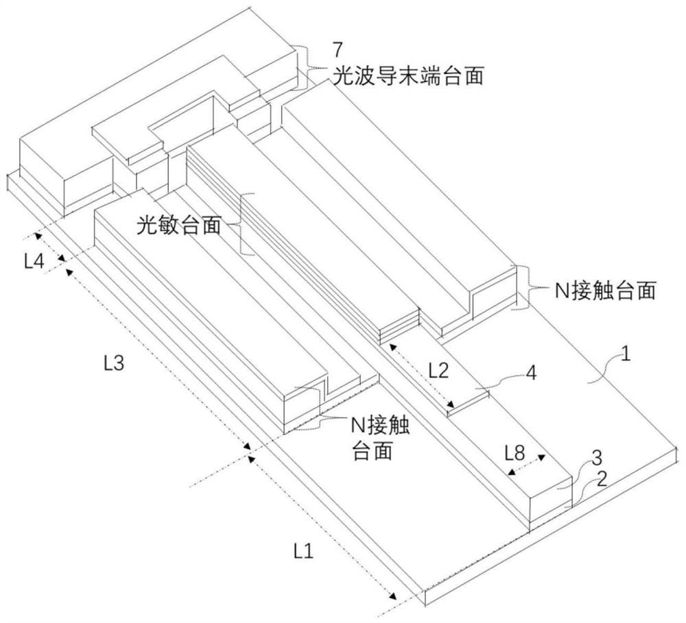
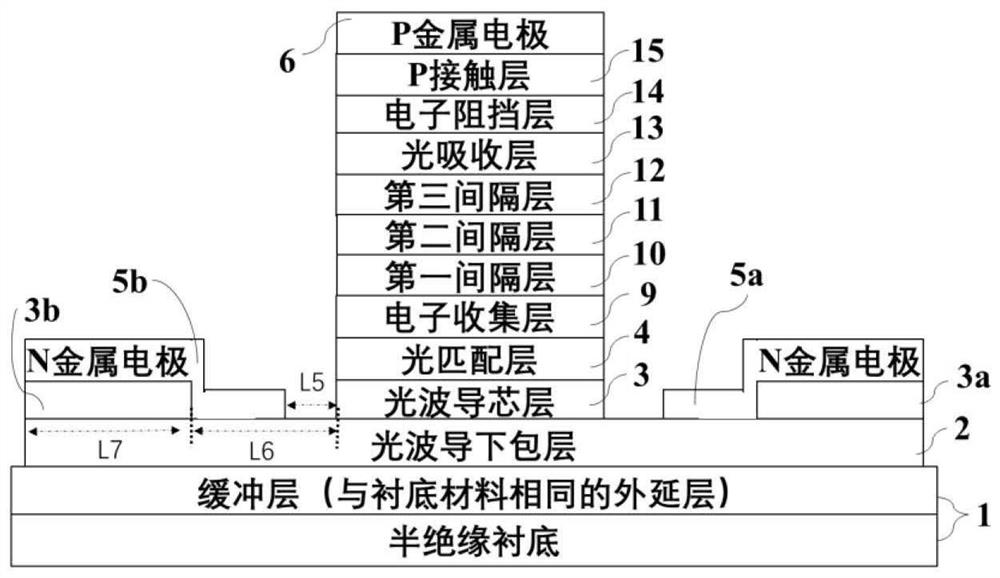
[0019] see figure 1 The three-dimensional schematic diagram of the device and figure 2The schematic diagram of the cross-section of the active region perpendicular to the light incident direction is shown. As a specific embodiment, the low-powe...


PUM

PropertyMeasurementUnit
thicknessaaaaaaaaaa
thicknessaaaaaaaaaa
thicknessaaaaaaaaaa

Abstract

The invention claims to protect a low-power-consumption waveguide photodetector structure with optical isolation between the photosensitive mesa and the N-contact mesa. The structure integrates the light waveguide and the photodiode on a semi-insulating substrate. Among them, the photodiode has an optimized energy band structure, doping distribution and epitaxial layer thickness, mainly including a non-depleted P-type light absorption layer with a linear gradient doping distribution, and an N-type electron collection layer (non-depleted) with a linear gradient doping distribution. light absorbing layer), and a graded bandgap spacer layer with a sandwich dipole doping profile between the absorbing layer and the collecting layer. By making a groove on the N mesa and depositing a metal thin film electrode to optically isolate the photosensitive mesa from the N contact mesa, thereby improving the light confinement of the optical waveguide; making a mesa isolated from the N mesa at the end of the optical waveguide and depositing The upper metal thin film is used as a light reflector to increase the effective absorption length of the device, which is a technical solution to alleviate the mutual restriction between the bandwidth of the photodetector and the quantum efficiency.

Description

technical field [0001] The invention belongs to the technical fields of optical communication and optoelectronics, and in particular relates to a low-power-consumption waveguide photodetector structure with optical isolation between a photosensitive table and an N-contact table. Background technique [0002] Photodetectors with high quantum efficiency, broadband and high output power are key components in optical communication systems. In general, there is a mutually restrictive relationship between the bandwidth and quantum efficiency of photodetectors. The two main bandwidth limiting factors in photodetectors are carrier transit time and RC time. By reducing the device area or increasing the thickness of the depletion layer, the junction capacitance can be reduced to alleviate the RC time limit. However, increasing the thickness of the depletion layer, especially the thickness of the depleted absorber layer, will increase the carrier transit time. On the other hand, red...

Claims


Application Information

Patent Timeline
Patent Type & Authority Patents(China)
IPC IPC(8): H01L31/0232H01L31/0352H01L31/102
CPCH01L31/02327H01L31/035281H01L31/102
Inventor 刘涛马勇王玺
Owner CHONGQING UNIV OF POSTS & TELECOMM
Why Eureka
Try Eureka