Medium pressurized thermal annealing mixed bonding method

A technology of thermal annealing and hybrid bonding, which is used in the manufacture of electrical components, electrical solid-state devices, semiconductor/solid-state devices, etc.

Inactive Publication Date: 2015-12-09
WUHAN XINXIN SEMICON MFG CO LTD
View PDF4 Cites 15 Cited by
  • Summary
  • Abstract
  • Description
  • Claims
  • Application Information

AI Technical Summary

Problems solved by technology

[0007] The purpose of the present invention is to provide a hybrid bonding technology to solve the problem of bonding failure in the thermal annealing process due to differences in thermal expansion coefficients in the hybrid bonding technology

Method used


Image

  • Medium pressurized thermal annealing mixed bonding method
  • Medium pressurized thermal annealing mixed bonding method
  • Medium pressurized thermal annealing mixed bonding method

Examples


Embodiment Construction

[0021] The principles and features of the present invention are described below in conjunction with the accompanying drawings, and the examples given are only used to explain the present invention, and are not intended to limit the scope of the present invention.

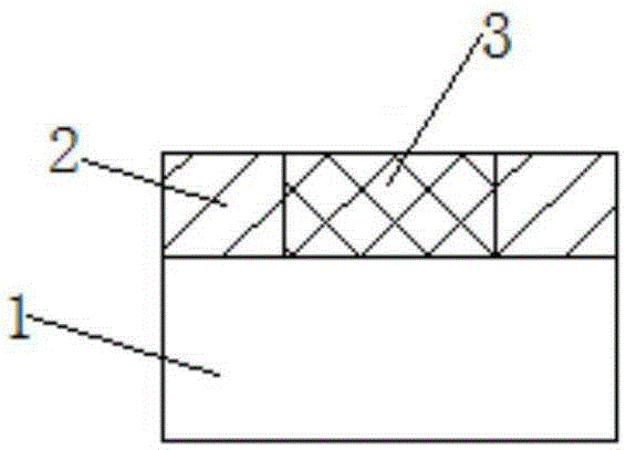
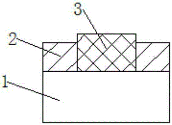
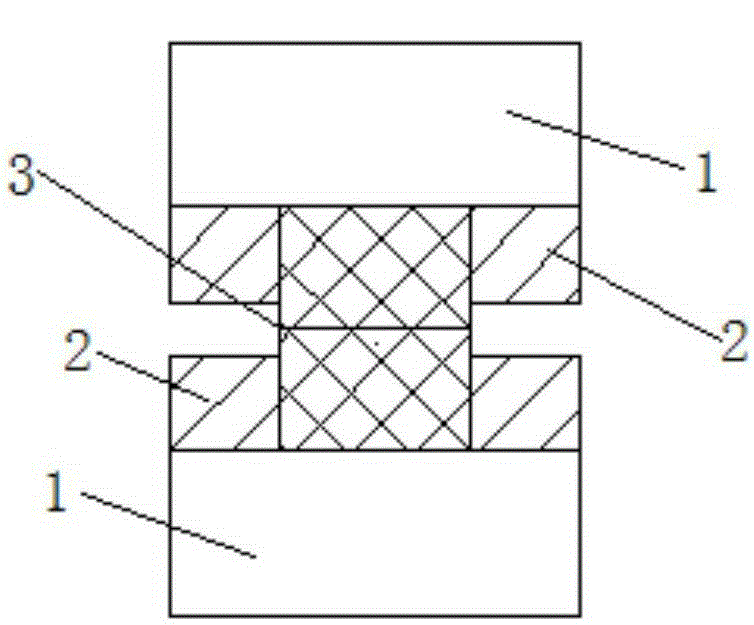
[0022] A medium pressurized mixed bonding method of the present invention, after the mixed bond is completed at normal temperature and pressure, special medium pressurized thermal annealing is carried out: in the thermal annealing environment, a medium with good thermal conductivity is used to bond the bonded The wafer exerts pressure, and at the same time as the thermal annealing is completed, the pressure is used to offset the internal pressure generated by the thermal expansion on the wafer interface; thus weakening the influence of the difference in the thermal expansion coefficient of different media on the wafer surface.

[0023] The specific embodiments of the present invention will be further described below ...


PUM


Abstract

The invention relates to a medium pressurized thermal annealing mixed bonding method, which comprises following steps: after completing the mixed bonding under normal temperature and pressure, special medium pressurized thermal annealing is carried out; under the thermal annealing environment, a medium with good thermal conductivity is used to apply pressure on wafers that are bonded; and at the time of completing the thermal annealing, pressure is used to counteract the internal pressure generated by the thermal expansion on the wafer interfaces, thus the influence of thermal expansion coefficient differences of different mediums on the wafer surfaces is weakened. By adopting the method provided herein, the influence of the differences of the thermal expansion coefficient between metal on the mixed bonding interface and insulating substance is weakened, thus the successful bonding rate is improved; and at the same time, the limitation of the design of the mixed bonding technology is improved, for example, the area ratio of different thermal expansion coefficient substances on the interface is not needed to be taken into account.

Description

technical field [0001] The invention relates to the field of semiconductor manufacturing, in particular to a medium pressurized thermal annealing hybrid bonding method. Background technique [0002] As the development of VLSI is approaching the physical limit, 3D integrated circuits, which have advantages in both physical size and cost, are an effective way to extend Moore's Law and solve advanced packaging problems. The wafer bonding technology is one of the key technologies of three-dimensional circuit integration, especially the hybrid bonding technology can realize the internal interconnection of thousands of chips while bonding two wafers, which can greatly improve chip performance and save cost. Hybrid bonding technology refers to the bonding method in which metal and insulating substances exist simultaneously on the wafer bonding interface. [0003] Mixed bonding exists both metal and insulating substances on the interface. In the bonding technology, high temperatur...

Claims


Application Information

Patent Timeline
Patent Type & Authority Applications(China)
IPC IPC(8): H01L21/603H01L21/324
CPCH01L21/324H01L24/80H01L24/82H01L2224/82H01L2224/8212H01L2224/828
Inventor 梅绍宁程卫华陈俊朱继锋
Owner WUHAN XINXIN SEMICON MFG CO LTD
Why Eureka
Try Eureka