Display substrate, display device and manufacturing method for display substrate

A display substrate and display device technology, which is applied in the field of communication, can solve the problems of low light transmittance of display substrates, achieve the effect of increasing light transmittance and meeting the requirements of luminous flux

Active Publication Date: 2020-02-14
VIVO MOBILE COMM CO LTD
View PDF4 Cites 6 Cited by
  • Summary
  • Abstract
  • Description
  • Claims
  • Application Information

AI Technical Summary

Problems solved by technology

[0003] Embodiments of the present invention provide a display substrate, a display device, and a method for ma

Method used


Image

  • Display substrate, display device and manufacturing method for display substrate
  • Display substrate, display device and manufacturing method for display substrate
  • Display substrate, display device and manufacturing method for display substrate

Examples


Example Embodiment

[0019] The technical solutions in the embodiments of the present invention will be clearly and completely described below in conjunction with the accompanying drawings in the embodiments of the present invention. Obviously, the described embodiments are part of the embodiments of the present invention, rather than all of them. Based on the embodiments of the present invention, all other embodiments obtained by those of ordinary skill in the art without creative work shall fall within the protection scope of the present invention.

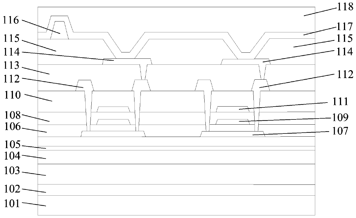
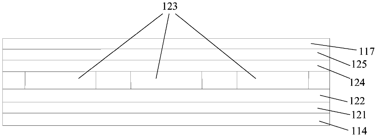
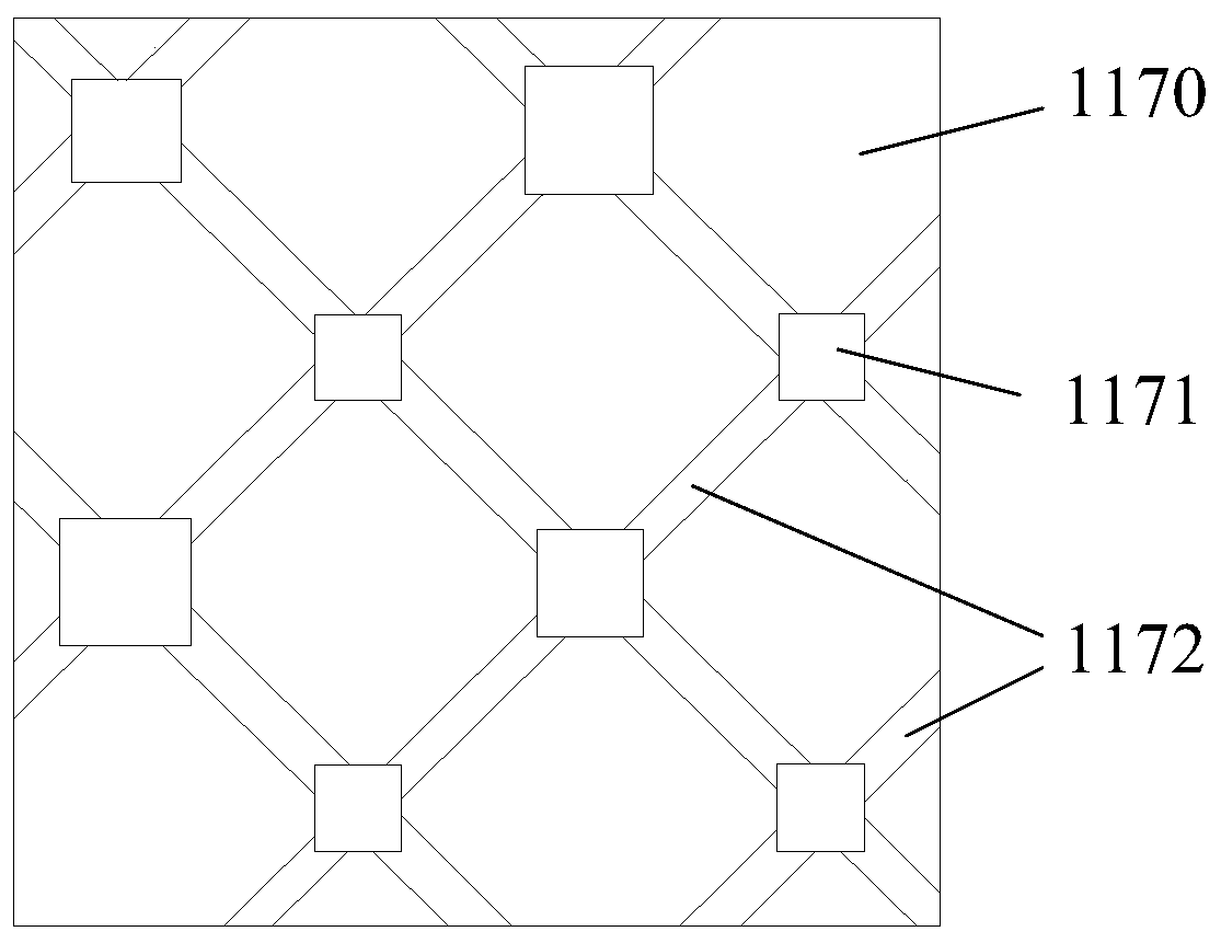
[0020] The embodiment of the present invention provides a display substrate, please refer to Figure 1 to Figure 4 The display substrate includes a base substrate 101, a first electrode layer 114, and a second electrode layer 117. The first electrode layer 114 is located between the base substrate 101 and the second electrode layer 117, and the second electrode layer 117 includes a light-transmitting layer. The light-transmitting area includes multiple...


PUM


Abstract

The invention provides a display substrate, a display device and a manufacturing method for the display substrate. The display substrate comprises a substrate, a first electrode layer and a second electrode layer, wherein the first electrode layer is located between the substrate and the second electrode layer; the second electrode layer comprises a light-transmitting region; the light-transmitting region comprises a plurality of pattern islands and a plurality of inter-island connecting lines; every two adjacent pattern islands are electrically connected through the inter-island connecting lines; the areas, except the pattern islands and the inter-island connecting lines, in the light-transmitting region are hollowed-out regions; and the orthographic projections of the pattern islands onthe first electrode layer cover the electrodes of the first electrode layer. According to the technical scheme, the problem that an existing display substrate is low in light transmittance is solved.

Description

technical field [0001] The present invention relates to the field of communication technology, in particular to a display substrate, a display device and a manufacturing method of the display substrate. Background technique [0002] With the rapid development of science and technology, the photosensitive module under the screen has become one of the main development trends of terminal equipment. In order to ensure the photosensitive effect of the photosensitive module, the photosensitive module under the screen needs the photosensitive sensor to receive sufficient luminous flux within a limited time. However, the current design of the display substrate has the problem of low light transmittance. Contents of the invention [0003] Embodiments of the present invention provide a display substrate, a display device, and a manufacturing method of the display substrate, so as to solve the problem of low light transmittance of the existing display substrate. [0004] In order t...

Claims


Application Information

Patent Timeline
IPC IPC(8): H01L27/32
CPCH10K59/65H10K59/123H10K59/1213H10K59/1315
Inventor 熊建清
Owner VIVO MOBILE COMM CO LTD
Why Eureka
Try Eureka