Array substrate, display panel and display device

A technology of array substrate and substrate substrate, which is applied to identification devices, static indicators, instruments, etc., can solve the problems of limited test area and inability to meet test requirements, and achieve the effect of reducing the number of

Active Publication Date: 2020-03-06
SHANGHAI AVIC OPTOELECTRONICS
View PDF10 Cites 17 Cited by
  • Summary
  • Abstract
  • Description
  • Claims
  • Application Information

AI Technical Summary

Problems solved by technology

[0005] In view of this, an embodiment of the present invention provides an array substrate, a display panel, and a display device to solve the problem that the testing requirements cannot be met due to the limited testing area.

Method used


Image

  • Array substrate, display panel and display device
  • Array substrate, display panel and display device
  • Array substrate, display panel and display device

Examples


Embodiment Construction

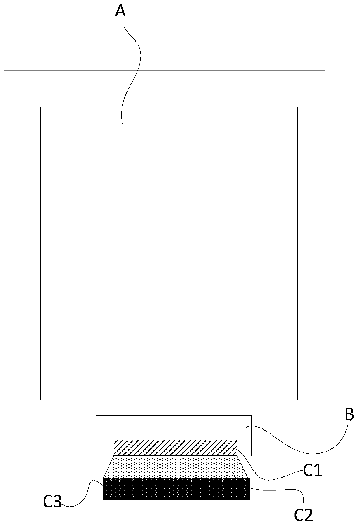
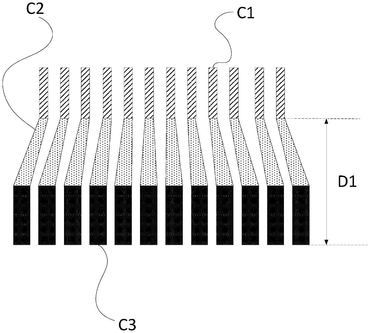
[0030] In the array substrate in the related art, such as figure 1 As shown, including the display area A, and the first binding area B for binding the driver chip on one side of the display area A, the output pin C3 of the flexible circuit board bound to the driver chip is connected to the The input pin C1 of the driver chip is bound, and its specific structure is as follows figure 2 shown.

[0031] Depend on figure 2 It can be seen that the step width D1 occupied by the connecting lead C2 and the output pin C3 of the flexible circuit board is relatively large, which is not conducive to realizing a narrow frame of the display panel.

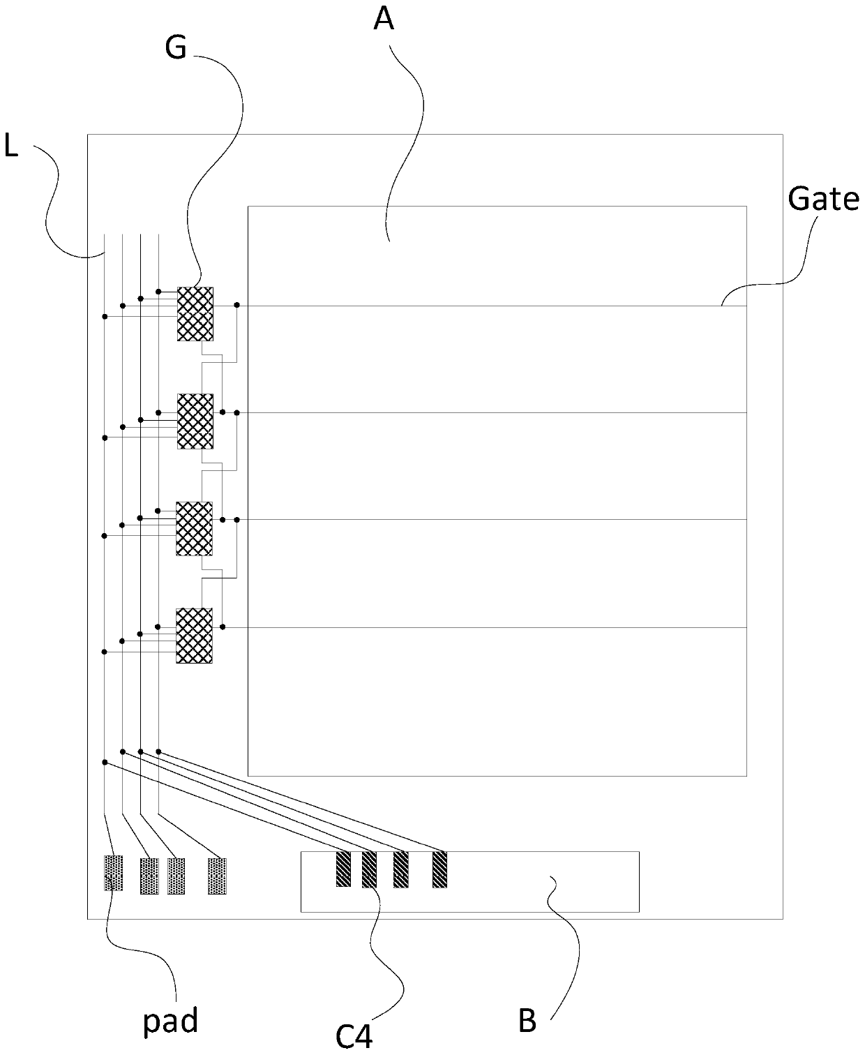
[0032] Among them, such as image 3 As shown, the first bonding area B also includes the output pin C4 of the driver chip, and the output pin C4 of the driver chip is used to provide electrical signals to the signal line L connected to the gate drive circuit G, so that the gate The electrode driving circuit G provides a signal to the corre...


PUM


Abstract

The invention discloses an array substrate, a display panel and a display device. The array substrate comprises a plurality of first potential signal lines and a plurality of second potential signal lines which are located in a peripheral region of a substrate baseplate; in the process of testing, what each of the plurality of first potential signal lines provides to a gate drive circuit is a first voltage signal, what each of the plurality of second potential signal lines provides to the gate drive circuit is a second voltage signal, therefore, the first voltage signals can be provided to theplurality of first potential signal lines through the same first test pad, and the second voltage signals are provided to the plurality of second potential signal lines through the same second test pad; and compared with the related art that each signal line connected with the gate drive circuit needs to be provided with a corresponding test pad, the number of the test pads can be greatly reduced, and the requirement for array substrate testing can be met even in a limited test area.

Description

technical field [0001] The present invention relates to the field of display technology, in particular to an array substrate, a display panel and a display device. Background technique [0002] With the development of display technology, people not only put forward higher requirements for the display quality of the display panel, but also put forward requirements for the screen ratio of the display area of ​​the display panel, which requires in-depth research on the narrow frame design of the display panel . [0003] The array substrate in the related art includes a display area and a driving chip binding area located on one side of the display area, and the flexible circuit board bound to the driving chip may be arranged on the side of the driving chip binding area away from the display area. However, since the lead wires and pins electrically connected to the flexible circuit board occupy a large step width, it is not conducive to the realization of a narrow frame; theref...

Claims


Application Information

Patent Timeline
Patent Type & Authority Applications(China)
IPC IPC(8): G09F9/30G09G3/00
CPCG09F9/30G09G3/006
Inventor 金慧俊王听海
Owner SHANGHAI AVIC OPTOELECTRONICS
Why Eureka
Try Eureka