Method for simulating power failure of memory in FPGA

A storage and memory technology, applied in the field of integrated circuit verification, can solve the problems of timing convergence difficulties, insufficient simulation of real states, etc., to achieve the effect of saving resources and meeting timing

Active Publication Date: 2020-04-28
成都华大九天科技有限公司
View PDF4 Cites 0 Cited by
  • Summary
  • Abstract
  • Description
  • Claims
  • Application Information

AI Technical Summary

Problems solved by technology

Although on FPGA, register resources are relatively abundant, but such consumption will be quite tight; second, need to utilize figure 1 A very large mux shown on the left side of the figure performs multi-level selection. This kind of multi-channel selection to the Nth power of 2 will introduce a very large data path delay in timing, plus the delay of the memory itself, It will be very difficult in timing closure
Third, when the data that has not been rewritten is read after the power failure is restored, its value can only be 0, which is not enough to simulate the real state of the memory after power failure

Method used


Image

  • Method for simulating power failure of memory in FPGA
  • Method for simulating power failure of memory in FPGA
  • Method for simulating power failure of memory in FPGA

Examples


Embodiment Construction

[0036] The preferred embodiments of the present invention will be described below in conjunction with the accompanying drawings. It should be understood that the preferred embodiments described here are only used to illustrate and explain the present invention, and are not intended to limit the present invention.

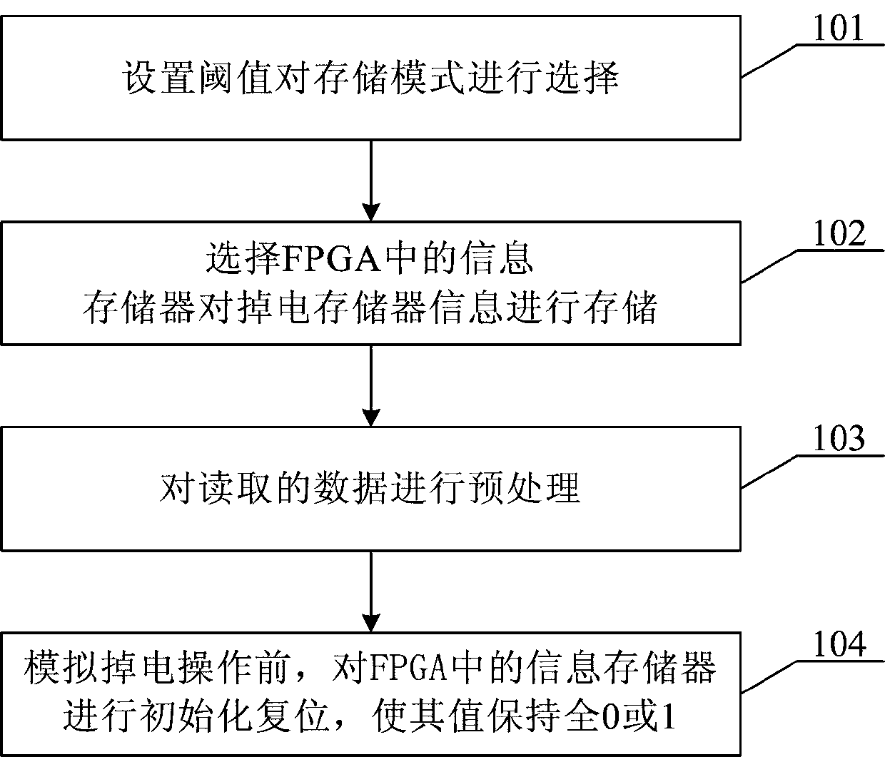
[0037] figure 1 For the method flowchart of simulating memory power-down in FPGA according to the present invention, below will refer to figure 1 , the method for simulating storage power-down in FPGA of the present invention is described in detail.

[0038] First, in step 101, a threshold is set to select a storage mode. In this step, when simulating the memory power-off, the user can first select a threshold to store the memory information through the FPGA memory; or the program automatically selects according to the size of the memory that needs power-off, for example If the number of memory addresses exceeds 1024, FPGA memory resources are used for storage. ...


PUM


Abstract

The invention discloses a method for simulating power failure of a memory in an FPGA (Field Programmable Gate Array). The method comprises the following steps: 1) selecting an information memory in the FPGA to store information of the power failure memory; 2) when the power-down memory is in a power-down state, sending a power-down signal to reset the information memory to the power-down state; 3)when the power-down memory is in write operation, updating address state information in the information memory; and 4) when the address state information in the information memory is 1, reading datawritten last time, otherwise, reading random data or 0. According to the method for simulating the power failure of the memory in the FPGA, rich memory resources on the FPGA are used for replacing information storage of a register, so that resources are saved, and the requirement of a time sequence is better met; the randomized operation is carried out at the data reading end, so that the power failure behavior can be simulated more truly.

Description

technical field [0001] The invention relates to the technical field of integrated circuit verification, in particular to a method for simulating memory power-off in FPGA. Background technique [0002] With the continuous development of ASIC design technology, more and more ASIC designs in recent years have adopted multi-voltage domain design for digital circuits. The design of multiple voltage domains enables the digital part to better meet the requirements of low power consumption. It plays a pivotal role in the design of current handheld devices or wireless headsets that are extremely sensitive to power consumption. [0003] However, current FPGAs have limited support for multi-voltage domains in the digital part, and some manufacturers do not even support this aspect. Among supported manufacturers, the processing of memory power-off will take up a lot of logic resources and lead to poor timing. [0004] figure 2 It is a method for simulating memory power-down in the p...

Claims


Application Information

Patent Timeline
Patent Type & Authority Applications(China)
IPC IPC(8): G06F11/26G06F30/20
CPCG06F11/261Y02D10/00
Inventor 刘小卫
Owner 成都华大九天科技有限公司
Why Eureka
Try Eureka