Bubble defect monitoring method and device, server and readable storage medium

A defect monitoring and bubble technology, used in electrical components, semiconductor/solid state device testing/measurement, circuits, etc., can solve the problems of inability to monitor millimeter-level bubbles, inability to monitor the shape of bubble defects, low detection accuracy, etc. The probability of bubble breaking, avoiding manual visual inspection, and high detection efficiency

Pending Publication Date: 2020-04-28
YANGTZE MEMORY TECH CO LTD
View PDF4 Cites 1 Cited by
  • Summary
  • Abstract
  • Description
  • Claims
  • Application Information

AI Technical Summary

Problems solved by technology

[0005] 1. Unable to monitor millimeter-level air bubble defects;
[0006] 2. The shape of bubble defects cannot be monitored
[0007] Therefore, the existing online air bubble defect monitoring system is almost ineffective in monitoring the air bubble defects in the bonded wafers. In the process, it is usua

Method used


Image

  • Bubble defect monitoring method and device, server and readable storage medium
  • Bubble defect monitoring method and device, server and readable storage medium
  • Bubble defect monitoring method and device, server and readable storage medium

Examples


Embodiment Construction

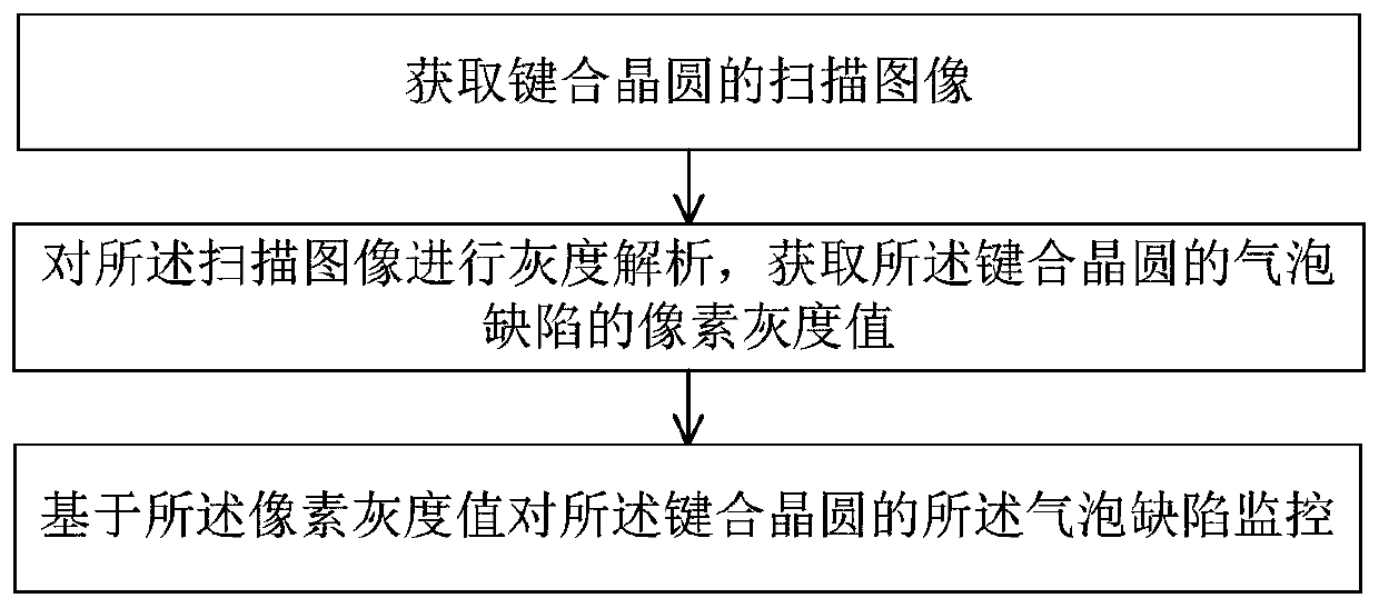
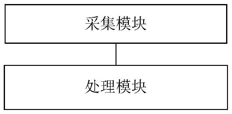
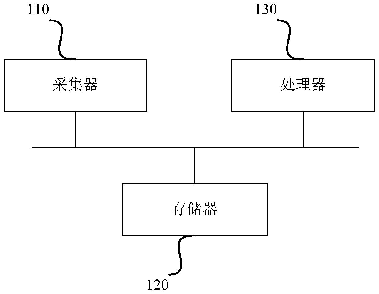
[0035] Embodiments of the present invention are described below through specific examples, and those skilled in the art can easily understand other advantages and effects of the present invention from the content disclosed in this specification. The present invention can also be implemented or applied through other different specific embodiments, and various modifications or changes can be made to the details in this specification based on different viewpoints and applications without departing from the spirit of the present invention.

[0036] see Figure 1 ~ Figure 3 . It should be noted that the diagrams provided in this embodiment are only schematically illustrating the basic idea of ​​the present invention, and only the components related to the present invention are shown in the diagrams rather than the number, shape and shape of the components in actual implementation. Dimensional drawing, the type, quantity and proportion of each component can be changed arbitrarily d...


PUM


Abstract

The invention provides a bubble defect monitoring method and device, a server and a readable storage medium. According to the bubble defect monitoring method and device, the server and the readable storage medium, gray analysis is performed on the scanning image of a bonded wafer, so that the pixel gray value of bubble defects is obtained; and therefore, the bubble defects can be monitored throughthe pixel gray value. With the bubble defect monitoring method and device, the server and the readable storage medium of the invention adopted, the size, shape and number of the bubble defects can beautomatically monitored on line; a manual visual inspection mode can be avoided; detection efficiency is high, accuracy is high; reliability is good; a bubble breaking probability is reduced; economic loss is reduced; production efficiency is improved; and relatively high economic value is realized.

Description

technical field [0001] The invention belongs to the technical field of semiconductor manufacturing, and relates to a bubble defect monitoring method, device, server and readable storage medium. Background technique [0002] In the wafer bonding (Bond) process, when there is an abnormality in the bonding process, bubble defects will appear in the bonded wafer. Once the size of the bubble defect reaches the millimeter level, the bonded wafer will not There may be a risk of bubbles bursting, and the shape of the bubble defect is also an important indicator of the bubbles breaking. [0003] In the semiconductor manufacturing process, the bursting of the bubbles in the bonded wafer will not only reduce the yield of the wafer, but even cause the wafer to be scrapped in severe cases, and will also pollute the process equipment to further contaminate other wafers. Expanded the scope of influence, resulting in greater economic losses. Therefore, the bubble defect in the bonded wafe...

Claims


Application Information

Patent Timeline
IPC IPC(8): H01L21/66
CPCH01L22/12H01L22/24
Inventor 詹冬武潘玉妹
Owner YANGTZE MEMORY TECH CO LTD
Why Eureka
Try Eureka