Display panel and display device

A display panel and display area technology, which is used in identification devices, semiconductor/solid-state device components, instruments, etc., can solve problems such as affecting the display effect of the display panel, the display panel cannot be displayed normally, and affecting the working performance of electronic components.

Active Publication Date: 2020-05-08
KUNSHAN GO VISIONOX OPTO ELECTRONICS CO LTD
View PDF8 Cites 6 Cited by
  • Summary
  • Abstract
  • Description
  • Claims
  • Application Information

AI Technical Summary

Problems solved by technology

[0003] The display panel generally includes a display area and a non-display area arranged around the display area. The display area is provided with light-emitting elements for display and electronic components corresponding to the light-emitting elements. The presence of static electricity in the display area of ​​the display panel will affect the The working performance of light-emitting elements and electronic components corresponding to light-emitting elements will affect the display effect of the display panel and even cause the display panel to fail to display normally.

Method used


Image

  • Display panel and display device
  • Display panel and display device
  • Display panel and display device

Examples


Embodiment Construction

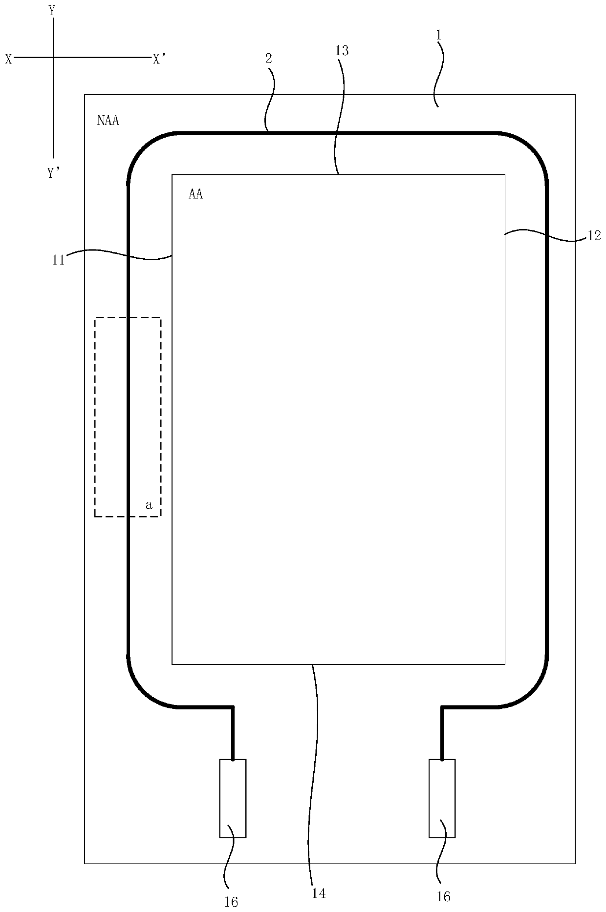
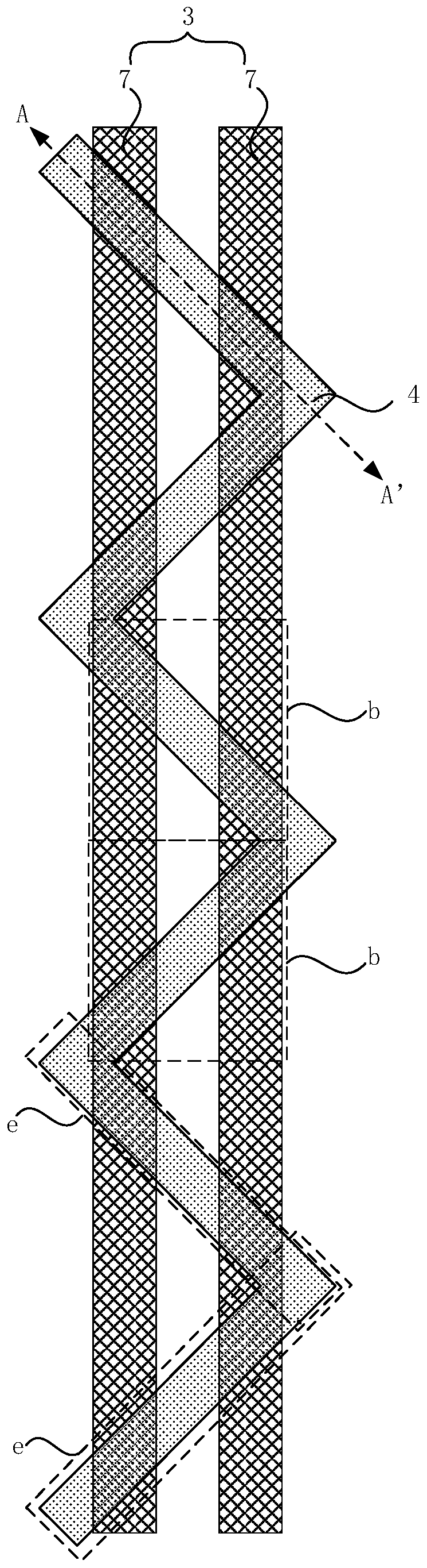
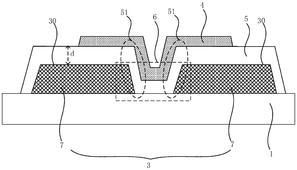
[0032] The present invention will be further described in detail below in conjunction with the accompanying drawings and embodiments. It should be understood that the specific embodiments described here are only used to explain the present invention, but not to limit the present invention. In addition, it should be noted that, for the convenience of description, only some structures related to the present invention are shown in the drawings but not all structures. Throughout this specification, the same or similar reference numerals represent the same or similar structures, elements or processes. It should be noted that, in the case of no conflict, the embodiments in the present application and the features in the embodiments can be combined with each other.

[0033] As in the background technology, a display panel generally includes a display area and a non-display area arranged around the display area. The display area of ​​the display panel is provided with light-emitting ...


PUM

PropertyMeasurementUnit
thicknessaaaaaaaaaa

Abstract

The invention discloses a display panel and a display device. The display panel comprises a substrate and an electrostatic protection structure, wherein the electrostatic protection structure is located on the substrate; the electrostatic protection structure is arranged around at least part of a display area of the display panel; the electrostatic protection structure comprises at least two layers of patterned structures, namely, a first patterned structure and a second patterned structure; the second patterned structure is located on the side, which is away from the substrate, of the first patterned structure; the first patterned structure and the second patterned structure are arranged on adjacent metal layers respectively; and a dielectric layer is arranged between the first patternedstructure and the second patterned structure; in the direction perpendicular to the display panel, the first patterned structure and the second patterned structure have at least one overlapping area;an acute included angle is formed between the extending direction of the first patterned structure and the extending direction of the second patterned structure in the overlapping area; and the firstpatterned structure is provided with a concave part corresponding to the overlapping area. According to the technical scheme, the antistatic capacity of the electrostatic protection structure is optimized.

Description

technical field [0001] Embodiments of the present invention relate to the field of display technology, and in particular, to a display panel and a display device. Background technique [0002] With the development of display technology, more and more display devices are applied to people's daily life and work, which brings great convenience to people's daily life and work. Static electricity exists widely in daily life and work. During the use of the display device, Electro Static Discharge (EDS) is a necessary means to avoid failure of the display device. [0003] The display panel generally includes a display area and a non-display area arranged around the display area. The display area is provided with light-emitting elements for display and electronic components corresponding to the light-emitting elements. The presence of static electricity in the display area of ​​the display panel will affect the The working performance of the light-emitting element and the electroni...

Claims


Application Information

Patent Timeline
Patent Type & Authority Applications(China)
IPC IPC(8): H01L23/60H01L27/32G09F9/33
CPCH01L23/60G09F9/33H10K59/12
Inventor 常苗张露朱修剑张金方胡思明韩珍珍
Owner KUNSHAN GO VISIONOX OPTO ELECTRONICS CO LTD
Why Eureka
Try Eureka