
Thin-film transistor array substrate and mending method thereof

A technology of thin-film transistors and substrates, which is applied in the field of active component array substrates and their repairs, can solve problems such as poor display quality, false conduction, and pixel unit failure to display normally in liquid crystal displays, so as to improve the failure of normal display and increase the yield rate of the process Effect

Active Publication Date: 2008-04-09
AU OPTRONICS CORP
View PDF5 Cites 0 Cited by
  • Summary
  • Abstract
  • Description
  • Claims
  • Application Information

AI Technical Summary

Problems solved by technology

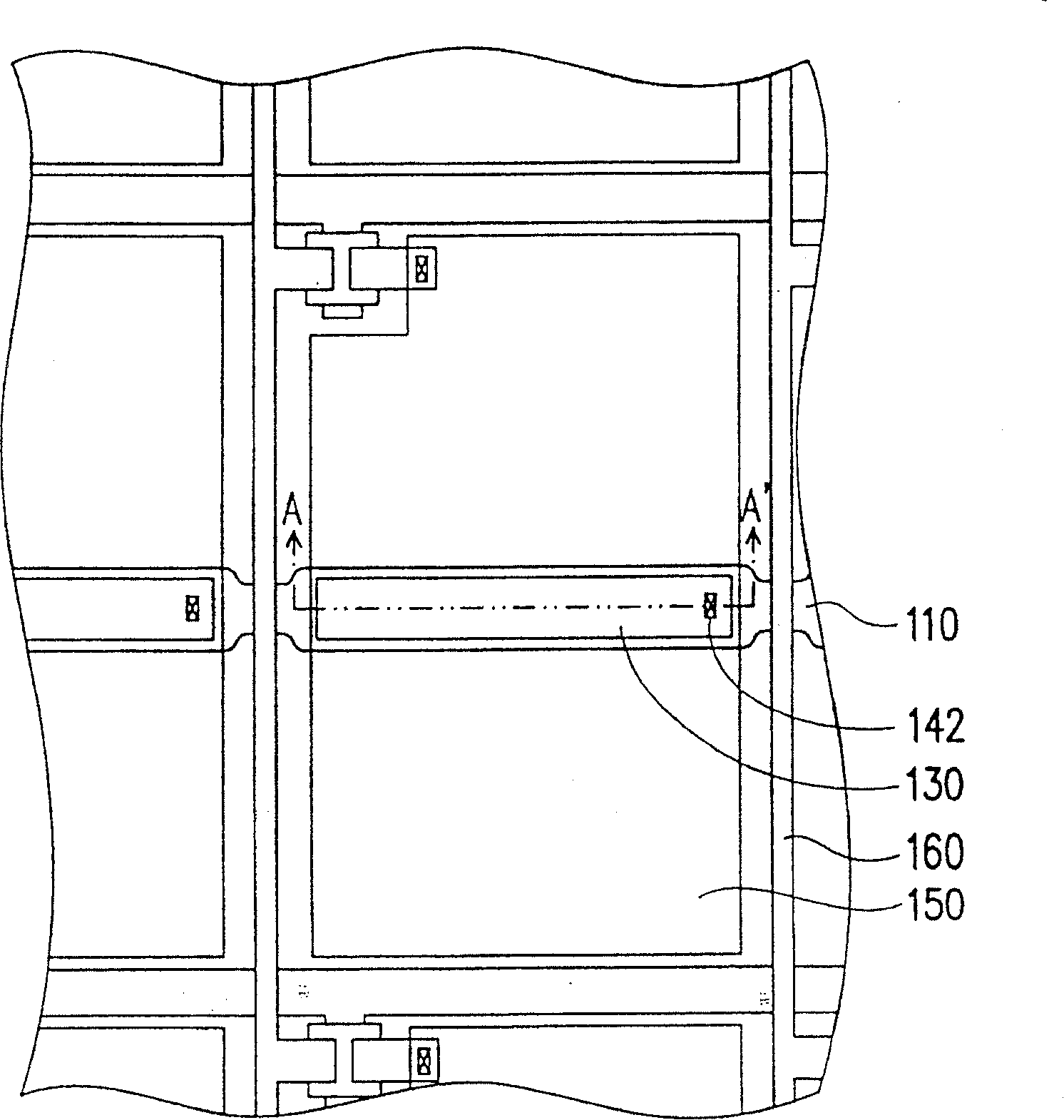
In addition, if Figure 3A and Figure 3B As shown, when making the data wiring 160 and the upper electrode 130 in the past, there may be some conductive material 170 (such as aluminum) left between the data wiring 160 and the upper electrode 130, so that the pixel electrode 150 passes through the upper electrode 130. False conduction with data wiring 160
Additionally, if Figure 4A and Figure 4B As shown, when manufacturing the pixel electrodes 150, the residue of the conductive material 180 (such as indium tin oxide, ITO) may also occur between the adjacent pixel electrodes 150, so that the adjacent pixel electrodes 150 are misconducted.
Wherein, regardless of the above circumstances, the pixel unit cannot display normally, thus resulting in poor display quality of the liquid crystal display.

Method used


Image

  • Thin-film transistor array substrate and mending method thereof
  • Thin-film transistor array substrate and mending method thereof
  • Thin-film transistor array substrate and mending method thereof

Examples


Embodiment Construction

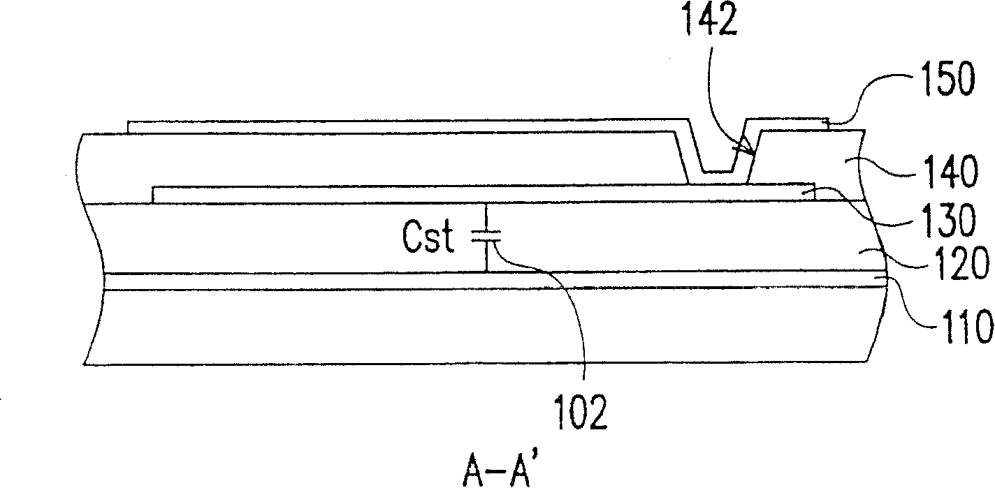
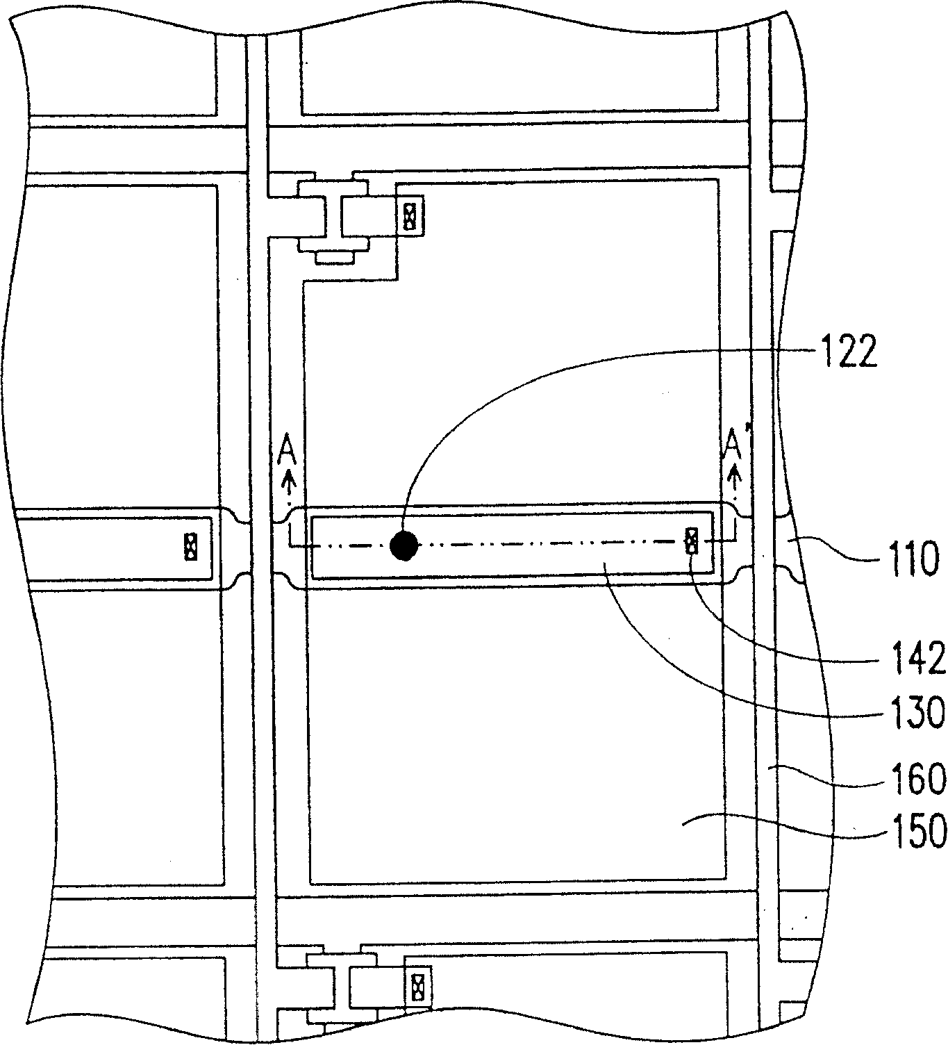
[0045] Please refer to Figure 5A and 5B ,in Figure 5A It is a partial top view of a thin film transistor array substrate of the present invention, and Figure 5B shown as Figure 5A B-B' sectional view, wherein the thin film transistor array substrate is suitable for a multi-region vertical alignment liquid crystal display panel, for example. Such as Figure 5A and 5B As shown, the substrate 500 is, for example, a glass substrate on which, for example, a plurality of scanning wirings 502 and a plurality of data wirings 504 are arranged to divide a plurality of pixel regions 500 a on the substrate 500 . In addition, a plurality of shared wires 506 are arranged on the substrate 500, which are formed simultaneously with the scan wires 502, and are made of a metal with good conductivity such as chromium (Cr) or aluminum (Al), and each shared wire The wiring 506 is located in the corresponding pixel area 500a.

[0046] please refer again Figure 5A and Figure 5B For exa...


PUM


Abstract

It is a thin film transistor group base plate and its amending method, wherein the group comprises one base plate, multiple scanning lines, multiple material aligning lines, multiple sharing aligning lines and multiple picture element units. Each picture element unit comprises one thin film transistor, one picture element electrode, one upper electrode and one guide wire, wherein the picture element electrode is set on the relative sharing aligning lines top; the top electrode is set between the picture element electrode and its relative sharing aligning lines; the guide wire is set out of the sharing aligning lines and is coupled with the picture element electrode.

Description

technical field [0001] The invention relates to an active component array substrate and its repair method, and in particular to a thin film transistor array substrate and its repair method. Background technique [0002] A thin film transistor liquid crystal display (TFT LCD) is mainly composed of a thin film transistor array substrate, a color filter array substrate and a liquid crystal layer. The thin film transistor array substrate is composed of a plurality of thin film transistors arranged in an array, and each thin film transistor corresponds It is composed of configured pixel electrodes. Thin film transistors are used as switching components of pixel units, and in order to control individual pixel units, a specific pixel unit is usually selected through a scan line (scanline) and a data line (date line) coupled with the thin film transistor, Appropriate operating voltage is applied thereto to display the display data corresponding to the pixel unit. [0003] Existing...

Claims


Application Information

Patent Timeline
Patent Type & Authority Patents(China)
IPC IPC(8): H01L27/02H01L21/77G02F1/136
Inventor 黄韦凯陈奕任蔡承勋王炯宾
Owner AU OPTRONICS CORP
Learn More