Array substrate and liquid crystal display panel

An array substrate and substrate technology, applied in nonlinear optics, instruments, optics, etc., can solve problems such as abnormal electrical performance and abnormal display of liquid crystal display panels, and achieve the effect of maintaining performance stability, avoiding functional abnormalities, and improving user experience.

Inactive Publication Date: 2020-05-29
SHENZHEN CHINA STAR OPTOELECTRONICS TECH CO LTD
View PDF10 Cites 4 Cited by
  • Summary
  • Abstract
  • Description
  • Claims
  • Application Information

AI Technical Summary

Problems solved by technology

Thin film transistors will experience abnormal electrical properties when they are squeezed by gap spacers for a long time, and eventually lead to abnormal display of liquid crystal display panels.

Method used


Image

  • Array substrate and liquid crystal display panel
  • Array substrate and liquid crystal display panel
  • Array substrate and liquid crystal display panel

Examples


Embodiment Construction

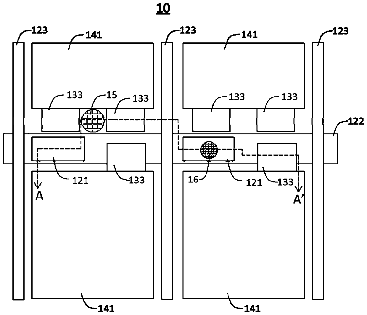
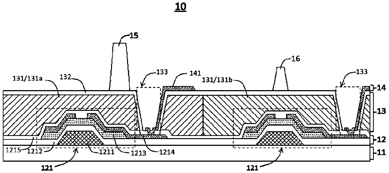
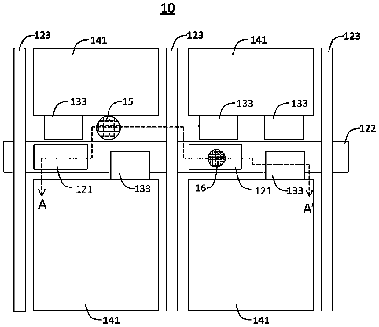
[0030] The following descriptions of the various embodiments refer to the accompanying drawings to illustrate specific embodiments in which the invention may be practiced. The directional terms mentioned in the present invention, such as [top], [bottom], [front], [back], [left], [right], [inside], [outside], [side], etc., are only for reference The orientation of the attached schema. Therefore, the directional terms used are used to illustrate and understand the present invention, but not to limit the present invention. In the figures, structurally similar elements are denoted by the same reference numerals.

[0031] An embodiment of the present application provides an array substrate, the array substrate includes a supporting first spacer, and the first spacer is vertically staggered from the thin film transistors on the array substrate, When the array substrate is used in a liquid crystal display panel, the downward force generated by the first spacer supporting the upper ...


PUM


Abstract

The invention provides an array substrate and a liquid crystal display panel. The array substrate comprises a substrate body, a thin film transistor layer and a color resistance layer arranged on thesubstrate body, a pixel electrode layer and a first spacer arranged on the color resistance layer, wherein the first spacer and a thin film transistor on the thin film transistor layer are arranged ina staggered mode in the vertical direction. The liquid crystal display panel comprises the array substrate. According to the liquid crystal display panel, the first spacers and the thin film transistors are arranged in the staggered mode in the vertical direction, the situation that the functions of the thin film transistors are abnormal due to the fact that the first spacers extrude the thin film transistors for a long time is avoided, the performance stability of the liquid crystal display panel can be maintained, and the use experience of a user is improved.

Description

technical field [0001] The invention relates to the field of display technology, in particular to an array substrate and a liquid crystal display panel. Background technique [0002] Liquid Crystal Display (LCD) has many advantages such as thin body, power saving, and no radiation, and is widely used in the field of display equipment. Currently common display devices, such as LCD TVs, mobile phones, computer monitors, notebook computers, etc., all have liquid crystal display technology. [0003] The structure of the liquid crystal display panel generally includes a backlight module (Backlight module), a thin film transistor array substrate (Thin Film Transistor Array Substrate), a color filter substrate (Color Filter Substrate), and a film arranged between the thin film transistor array substrate and the color filter substrate. Liquid Crystal Layer. A gap spacer is also provided between the array substrate and the color filter substrate, which is used to support the accomm...

Claims


Application Information

Patent Timeline
Patent Type & Authority Applications(China)
IPC IPC(8): G02F1/1339G02F1/1335G02F1/1362
CPCG02F1/133514G02F1/13394G02F1/136209G02F1/136286
Inventor 张子翔
Owner SHENZHEN CHINA STAR OPTOELECTRONICS TECH CO LTD
Why Eureka
Try Eureka