Stacked buck converters
A technology of electronic converters and capacitors, which is used in output power conversion devices, instruments, and the conversion of DC power input to DC power output, etc., can solve problems such as high cost and cost impact
- Summary
- Abstract
- Description
- Claims
- Application Information
AI Technical Summary
Problems solved by technology
Method used
Image

Examples
Embodiment Construction
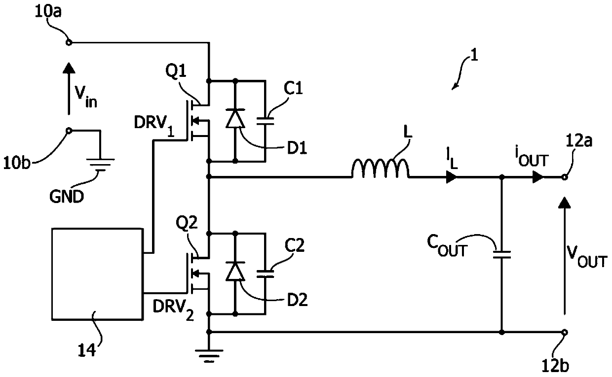
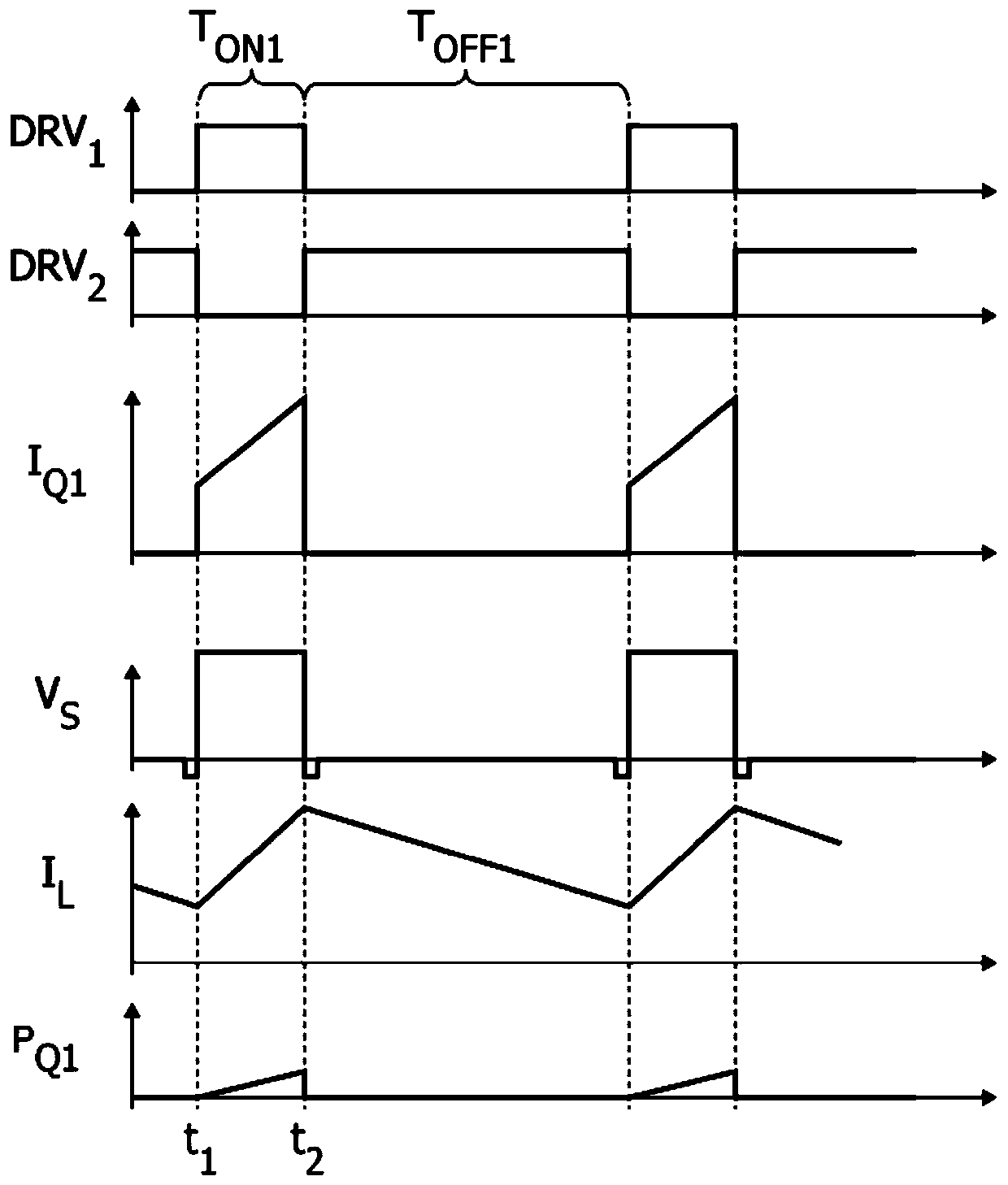
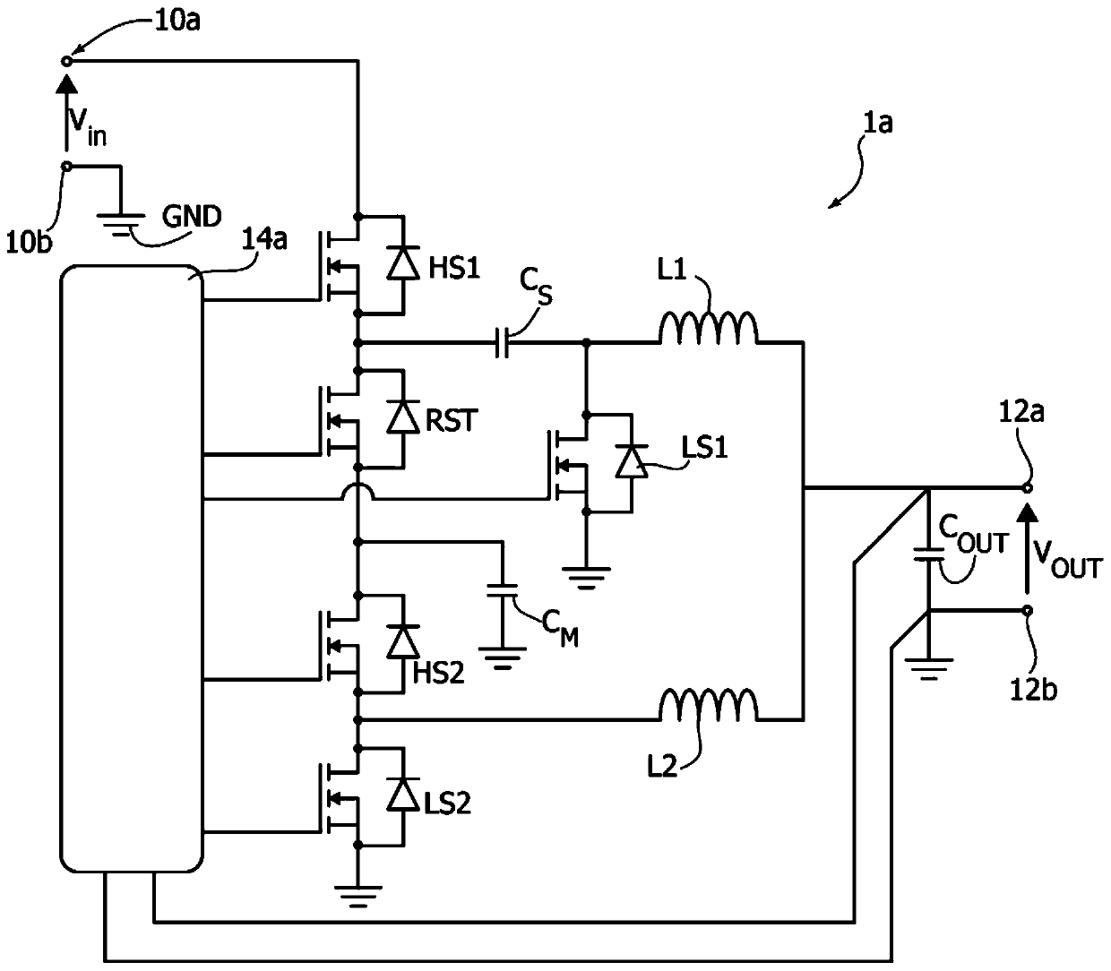
[0050] In the ensuing description, various specific details are shown in order to provide a thorough understanding of the embodiments. Embodiments may be obtained without one or more of the specific details, or using other methods, components, materials, etc. In other instances, known structures, materials, or operations are not shown or described in detail so as not to obscure aspects of the embodiments.
[0051] Within the framework of this specification, references to "an embodiment" or "one embodiment" are intended to indicate that a particular configuration, structure or characteristic described in connection with the embodiment is included in at least one embodiment. Thus, phrases such as "in an embodiment" or "in one embodiment" that may appear in various places in this specification do not necessarily refer to the same embodiment. Furthermore, particular configurations, structures or characteristics may be combined in any suitable manner in one or more embodiments.
...
PUM
 Abstract
Description
Claims
Application Information