A kind of microfluidic chip and using method thereof

A microfluidic chip, moving direction technology, applied in fluid controllers, chemical instruments and methods, laboratory containers, etc., can solve problems such as low optical detection efficiency, and achieve the effect of improving efficiency

Active Publication Date: 2022-06-03
BOE TECH GRP CO LTD +1
View PDF5 Cites 0 Cited by
  • Summary
  • Abstract
  • Description
  • Claims
  • Application Information

AI Technical Summary

Problems solved by technology

[0004] Embodiments of the present invention provide a microfluidic chip and a method of using the same to solve the problem of low optical detection efficiency of the microfluidic chip in the prior art

Method used


Image

  • A kind of microfluidic chip and using method thereof
  • A kind of microfluidic chip and using method thereof
  • A kind of microfluidic chip and using method thereof

Examples


Embodiment Construction

[0039] Aiming at the problem of low optical detection efficiency of the microfluidic chip in the prior art, an embodiment of the present invention provides a microfluidic chip and a method for using the same.

[0040] The specific implementation of the microfluidic chip provided by the embodiment of the present invention and its usage method will be described in detail below with reference to the accompanying drawings. The thickness and shape of each film layer in the drawings do not reflect the real scale, and the purpose is only to illustrate the content of the present invention.

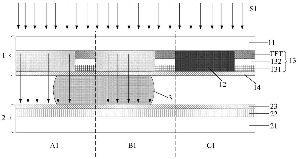
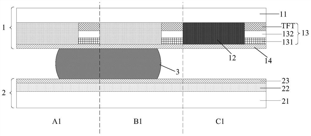
[0041] The microfluidic chip provided by the embodiment of the present invention, such as figure 1 As shown, it includes: a first substrate 1 and a second substrate 2 arranged oppositely;

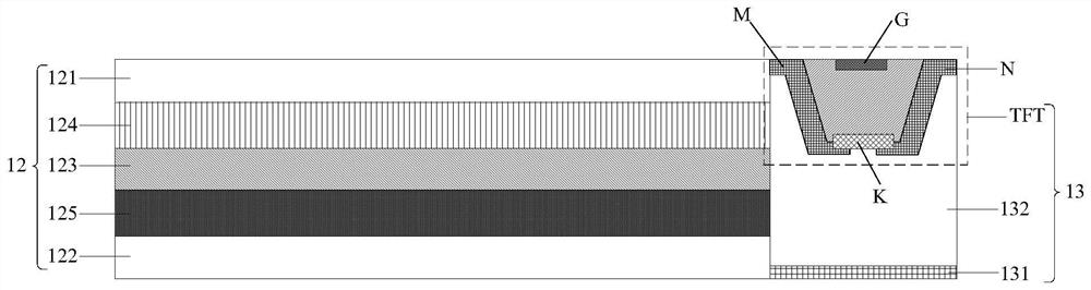
[0042] The first substrate 1 includes: a first base substrate 11, and a plurality of electrochromic structures 12 and drive circuits 13 located on the side of the first base substrate 11 facing the second subs...


PUM

PropertyMeasurementUnit
sizeaaaaaaaaaa

Abstract

The invention discloses a microfluidic chip and a method for using the same. The microfluidic chip includes: a first substrate and a second substrate oppositely arranged; the first substrate includes: a first base substrate, and a A plurality of electrochromic structures and driving circuits on the side of the base substrate facing the second substrate; there is a gap between the first substrate and the second substrate for accommodating liquid droplets; the driving circuit is used to control the liquid droplets during the detection stage The electrochromic structure at the position is light-transmitting, so that the external excitation light passes through the electrochromic structure and strikes the liquid droplet. By arranging a plurality of electrochromic structures and driving circuits in the first substrate, in the detection stage, the driving circuit can control the light transmission of the electrochromic structures at the position of the droplet, so that the external excitation light can pass through the electrochromic structures and emit light. To the liquid droplet, so as to drive the liquid droplet to generate fluorescence excitation, realize the optical detection of the liquid droplet at any position, and improve the efficiency of optical detection.

Description

technical field [0001] The invention relates to the technical field of trace detection, in particular to a microfluidic chip and a method for using the same. Background technique [0002] The laboratory on a chip can integrate the basic operation units such as sample preparation, reaction, separation, and detection in the biological, chemical, and medical analysis processes into a micron-scale chip, and automatically complete the entire analysis process. Due to the low cost of the laboratory on a chip, the detection time Short, high sensitivity and other advantages, has shown great prospects in the fields of biology, chemistry, medical reaction and separation. [0003] Among them, the microfluidic chip can automatically prepare and manipulate samples in the form of droplets. Optical detection can be used for sample detection. However, the magnitude of the optical signal generated by the sample is directly related to the intensity and accuracy of the excitation light. Relate...

Claims


Application Information

Patent Timeline
Patent Type & Authority Patents(China)
IPC IPC(8): B01L3/00G01N21/64
CPCB01L3/5027B01L3/502784B01L3/50273G01N21/6402B01L2400/0454
Inventor 樊博麟赵莹莹古乐姚文亮廖辉高涌佳李月
Owner BOE TECH GRP CO LTD
Why Eureka
Try Eureka