Method for safely and randomly switching working modes of chip and chip

A working mode and switching chip technology, which is applied in simulators, instruments, computer control, etc., can solve problems such as complex requirements and troublesome use of chips

Active Publication Date: 2020-07-14
四川中微芯成科技有限公司
View PDF21 Cites 0 Cited by
  • Summary
  • Abstract
  • Description
  • Claims
  • Application Information

AI Technical Summary

Problems solved by technology

In order to prevent unexpected state switching of the chip due to various reasons such as external interference in the normal working mode, in general, the requirements for entering the test or

Method used


Image

  • Method for safely and randomly switching working modes of chip and chip
  • Method for safely and randomly switching working modes of chip and chip
  • Method for safely and randomly switching working modes of chip and chip

Examples


Embodiment Construction

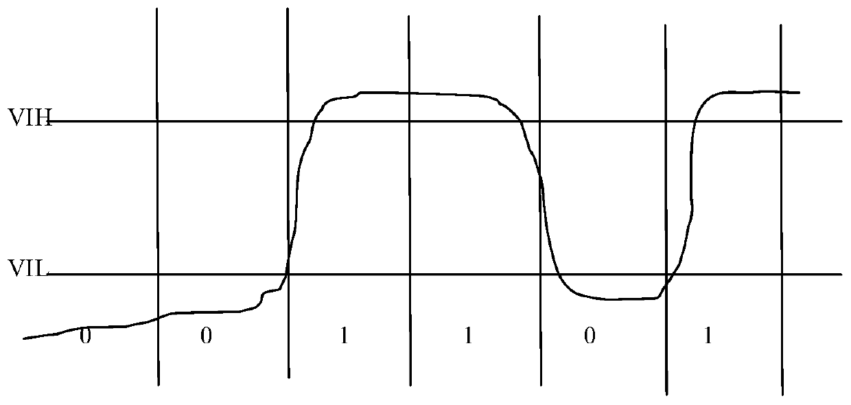
[0012] Existing switching circuits generally use digital analysis methods, which are vulnerable to external interference and wrong switching during work. Take sending 011101 signals to switch the normal working mode of the chip to the test mode as an example; figure 1 As shown, in the normal working mode, you want to send 001101 to the chip. When it is greater than VIH, it is judged as logic 1, and when it is less than VIL, it is judged as logic 0. When there are no interference factors, everything works normally, and the chip receives the signal of 001101.

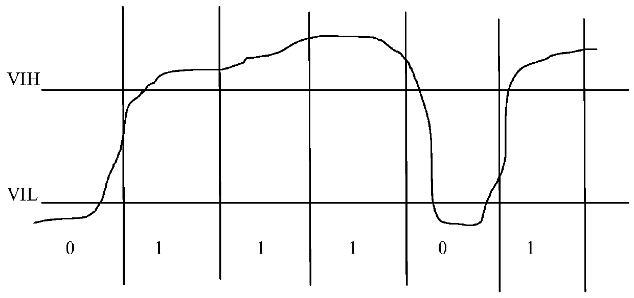
[0013] However, due to the interference of factors such as the environment, the voltage of the data signal changes, such as figure 2 As shown, due to the influence of interference, the voltage received by the chip fluctuates. In the second time slot, the voltage that should be less than VIL becomes greater than VIH. At this time, the second bit of the normal data signal 001101 is changed from 0 to 0 by mistake. It become...


PUM


Abstract

The invention relates to the field of integrated circuits, in particular to a method for randomly switching working modes of a chip and the chip in the field of microcontrollers. The system comprisesat least a first working mode and a second working mode. When the chip receives the first signal, the chip sends the second signal; the first working mode is switched to the second working mode, the first signal is analyzed by at least a first analysis mode and a second analysis mode, the first analysis mode is a digital signal analysis mode, the second analysis mode is an analog signal analysis mode, and the problems of working reliability and usability are solved.

Description

technical field [0001] The invention relates to the field of integrated circuits, in particular to a method and chip for arbitrarily switching chip working modes in the field of microcontrollers. Background technique [0002] As the functions of integrated circuits become more and more complex, the current basic circuit usually includes multiple working modes, one for normal work, and one or more modes for chip testing or chip programming. Various working modes require independent operation without interfering with each other, and can be switched freely. In order to prevent unexpected state switching of the chip due to various reasons such as external interference in the normal working mode, in general, the requirements for entering the test or programming mode are complicated, and it is difficult to directly switch to the testing or programming mode in the normal working mode , which brings unnecessary trouble to the use of the chip. Contents of the invention [0003] A...

Claims


Application Information

Patent Timeline
IPC IPC(8): G05B19/042
CPCG05B19/042G05B2219/25257
Inventor 胡泠朗
Owner 四川中微芯成科技有限公司
Why Eureka
Try Eureka