
Gate drive circuit and display device

A gate drive circuit and display device technology, applied to static indicators, instruments, etc., can solve problems such as unevenness, horizontal dense lines of display devices, etc., and achieve the effect of avoiding picture quality problems and uneven brightness and darkness

Inactive Publication Date: 2020-07-17
SHENZHEN CHINA STAR OPTOELECTRONICS TECH CO LTD
View PDF5 Cites 7 Cited by
  • Summary
  • Abstract
  • Description
  • Claims
  • Application Information

AI Technical Summary

Problems solved by technology

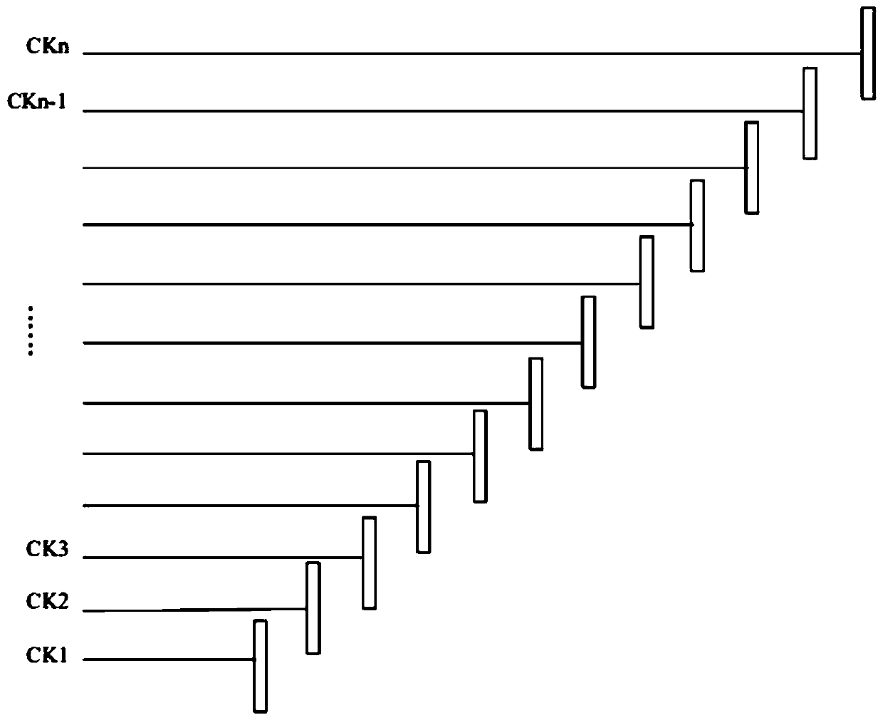
[0005] The purpose of the present application is to provide a gate drive circuit and a display device, to balance the falling time of the output scan signal of the gate drive unit connected to multiple clock signal lines in the gate drive circuit, and to avoid the capacitance difference of the clock signal lines from causing The display device has problems such as horizontal dense lines and uneven brightness and darkness, and while making full use of the free space of the two low-frequency AC signal lines, the two low-frequency AC signal lines have the same load

Method used


Image

  • Gate drive circuit and display device
  • Gate drive circuit and display device
  • Gate drive circuit and display device

Examples


Embodiment Construction

[0028] The technical solutions in the embodiments of the present application will be clearly and completely described below in conjunction with the drawings in the embodiments of the present application. Apparently, the described embodiments are only some of the embodiments of this application, not all of them. Based on the embodiments in this application, all other embodiments obtained by those skilled in the art without making creative efforts belong to the scope of protection of this application.

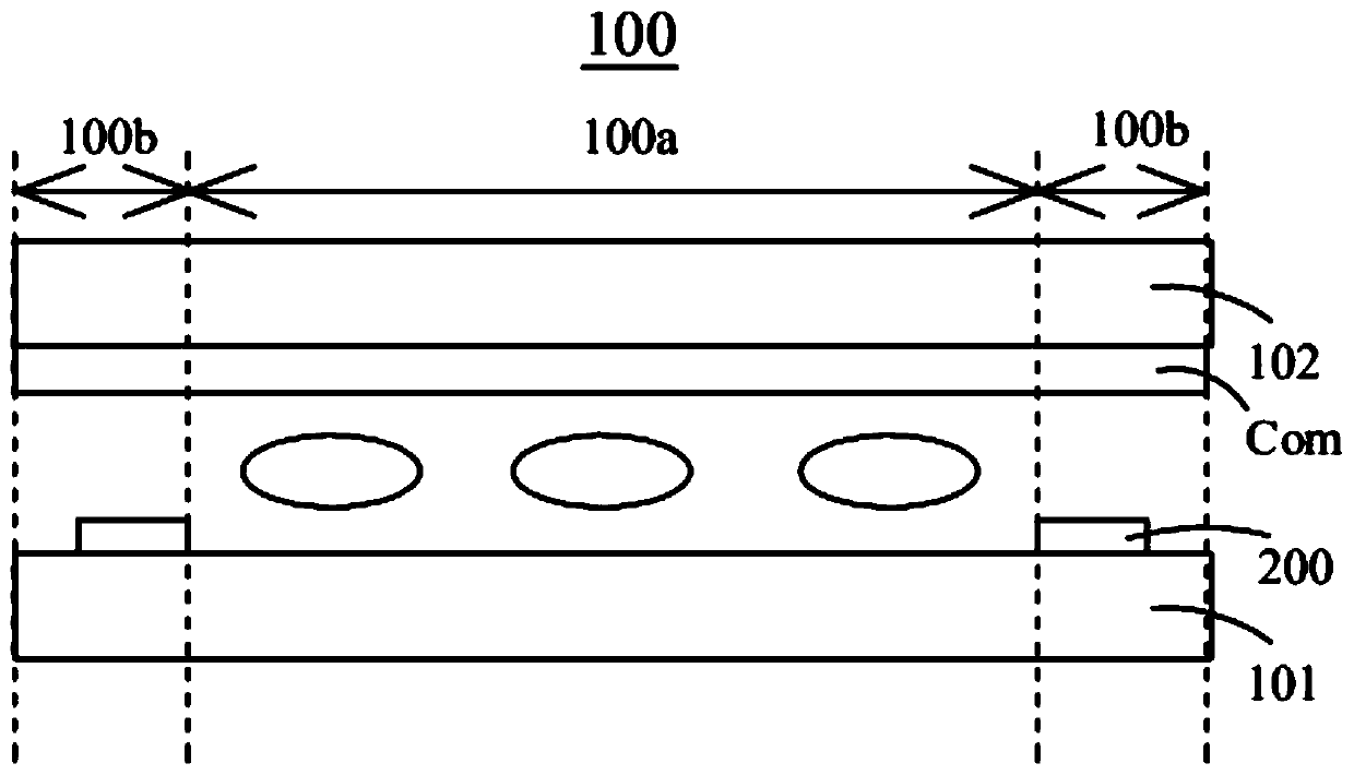
[0029] see figure 2 , which is a schematic diagram of a display device in an embodiment of the present application. The display device 100 includes an array substrate 101 , a color filter substrate 102 and a liquid crystal layer disposed between the array substrate 101 and the color filter substrate 102 .

[0030]The display device 100 has a display area 100a and a non-display area 100b located on the periphery of the display area 100a. The display area 100a is provided with ...


PUM


Abstract

The invention provides a gate drive circuit and a display device, and the gate drive circuit comprises two low-frequency AC signal lines which are used for transmitting low-frequency AC signals; and Nclock signal lines which are used for transmitting a clock signal, wherein the frequency of the clock signal is higher than that of the low-frequency AC signal, each clock signal line is provided with at least one capacitance compensation unit, the sum of the area of any clock signal line and the area of at least one capacitance compensation unit arranged on the same clock signal line is equal toa preset area, and N is an integer greater than or equal to 2, and wherein the at least one capacitance compensation unit arranged on each clock signal line comprises a first capacitance compensationunit arranged corresponding to at least one of the two low-frequency AC signal lines; the sum of the areas of the first capacitance compensation units arranged corresponding to one low-frequency AC signal line is equal to the sum of the areas of the first capacitance compensation units arranged corresponding to the other low-frequency alternating-current signal line.

Description

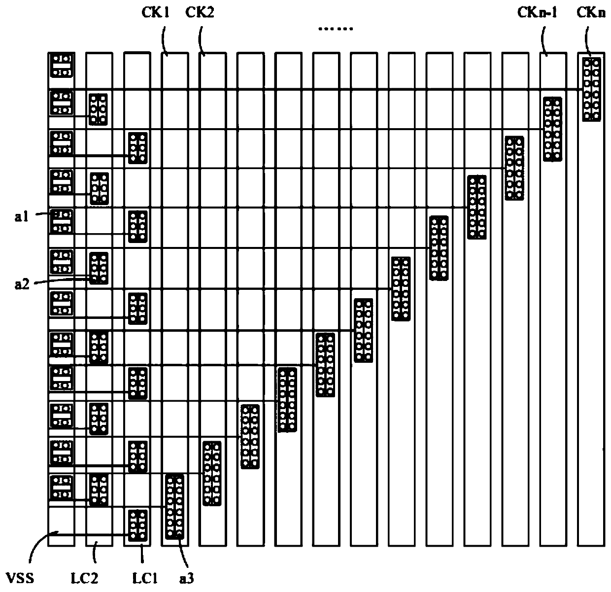
technical field [0001] The present application relates to the field of display technology, in particular to a gate drive circuit and a display device. Background technique [0002] At present, most gate driving circuits of a liquid crystal display (Liquid Crystal Display, LCD) adopt a design in which the gate driving circuit is arranged on a gate on array substrate (Gate On Array, GOA). The GOA circuit mainly includes a GOA busline circuit and a GOA unit circuit. The former refers to the wiring of each scan start signal and clock signal, and the latter refers to an independent unit including a complete GOA. [0003] Figure 1a is a schematic diagram of a traditional GOA wiring circuit, CK1-CKn are clock signal wiring, and n is 12. LC1 and LC2 are traces that provide low-frequency AC voltage signals to the pull-down sustaining unit of the GOA independent unit, and are reversed every 100 frames (Frame). VSS is a trace that provides a low potential DC voltage signal. a1-a3 a...

Claims


Application Information

Patent Timeline
Patent Type & Authority Applications(China)
IPC IPC(8): G09G3/36
CPCG09G3/3674
Inventor 陈亚妮
Owner SHENZHEN CHINA STAR OPTOELECTRONICS TECH CO LTD
Learn More