Display panel, display method thereof and display equipment
A display panel and display part technology, applied in the direction of instruments, electrical components, electric solid devices, etc., can solve the problems of inconsistency in brightness between the bending area and the flat area, and different display brightness, so as to solve the problem of inconsistency in brightness display and improve the intuitive experience Effect
- Summary
- Abstract
- Description
- Claims
- Application Information
AI Technical Summary
Problems solved by technology
Method used
Image
Examples
Embodiment 1
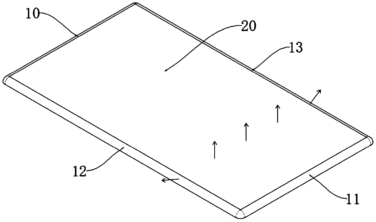
[0037] This embodiment provides a display panel, please refer to figure 1 , figure 1 It is a three-dimensional structural diagram of a display panel according to an embodiment of the present invention (the arrows in the figure are used to indicate the direction of light emission on the surface of the display panel when it is in operation). Specifically, the display panel includes a flat display portion 20 and a bent display portion at the edge of the flat display portion 20, and a thin film transistor is arranged in the display panel, specifically, a first thin film transistor is provided in the flat display portion 20, and a thin film transistor is provided in the flat display portion 20. There is a second thin film transistor in the display part, the ratio of the channel width W1 of the active layer of the first thin film transistor to the channel length L1 is the first set value W1 / L1, and the channel width of the active layer of the second thin film transistor is The rati...
Embodiment 2
[0045] Based on the same inventive concept as the first embodiment, this embodiment provides a display method of the display panel in the first embodiment, and the display method includes the following steps.
[0046] When the display panel is in normal operation, the ratio of the channel width to the channel length of the active layer of the second TFT is smaller than the ratio of the channel width to the channel length of the first TFT. The light emission intensity of the folded display portion is greater than that of the flat display portion 20 .
[0047] see Figure 5 , Figure 5 Schematic diagram of the potential change curve of the gate for driving the thin film transistor. During the entire process of the gate of the pixel electrode driving the thin film transistor, before the corresponding sub-pixel emits light, the potential of the gate for driving the thin film transistor can be divided into two Stage: the first stage is the gate potential reset stage, and the seco...
Embodiment 3
[0049] A display device, the display device may include the display panel of any structural form in Embodiment 1, and the display device may be an OLED display device, that is, this embodiment can provide a display panel with good display in the bending area at the edge of the screen. Effect of the OLED display, the display device provided by the present invention can be used in any electronic equipment with a display function such as mobile phones, tablet computers, televisions, notebook computers, and electronic paper book equipment. The above-mentioned OLED display device may be a PMOLED (Passive matrix OLED, passive matrix organic electroluminescent diode) display device, or an AMOLED (Active-matrix organic light-emitting diode, active matrix organic light-emitting diode) display device. Devices are often flexible display devices in specific applications.
PUM
| Property | Measurement | Unit |
|---|---|---|
| width | aaaaa | aaaaa |
| length | aaaaa | aaaaa |
| width | aaaaa | aaaaa |
Abstract
Description
Claims
Application Information


