Display panel
A display panel and display area technology, applied in static indicators, instruments, etc., can solve problems such as unfavorable panel narrow frame design, achieve the effect of solving bad display phenomenon, solving the problem of wide GOA area, and facilitating narrow frame design
- Summary
- Abstract
- Description
- Claims
- Application Information
AI Technical Summary
Problems solved by technology
Method used
Image

Examples
Embodiment 1
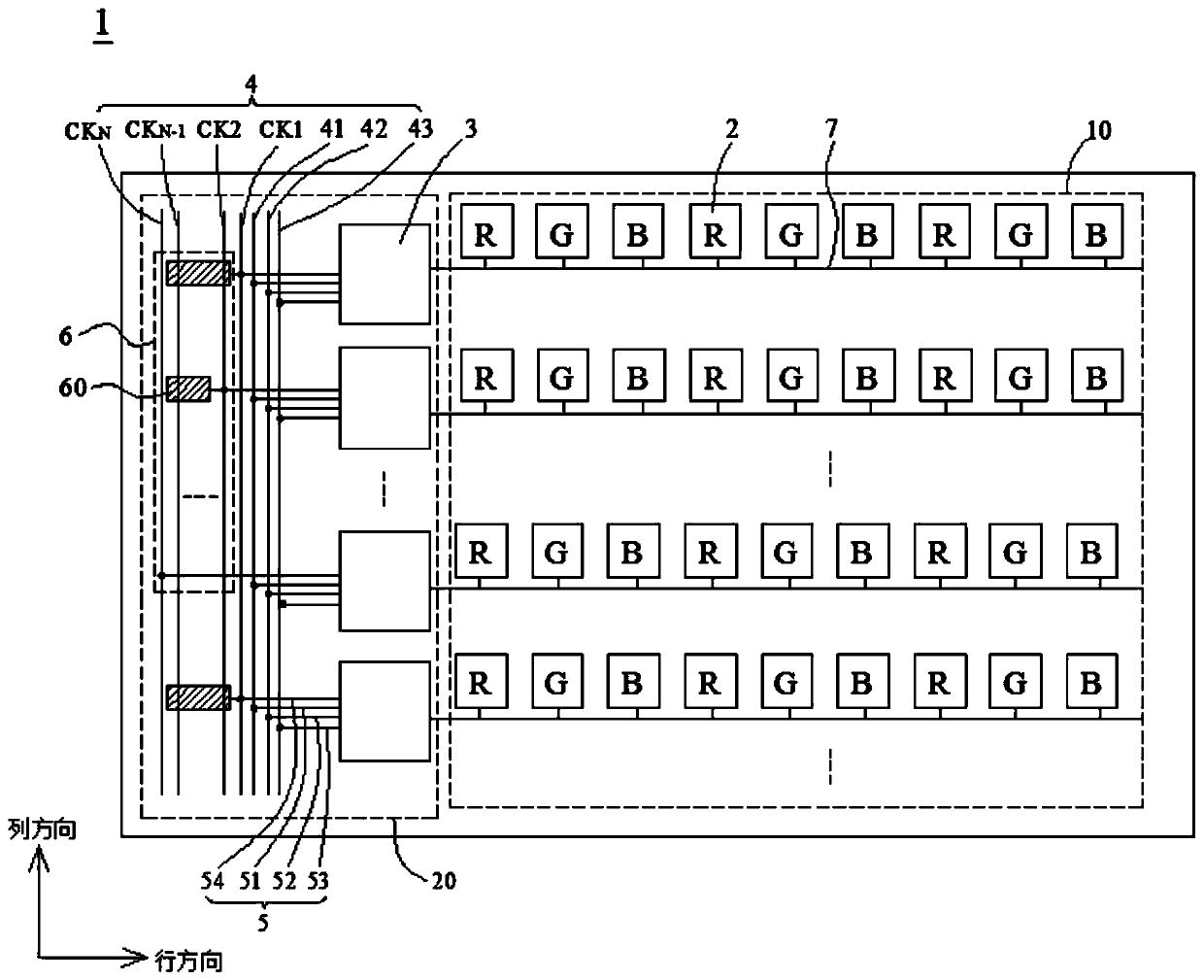
[0044] Please refer to figure 2 As shown in , it is a schematic structural diagram of the display panel provided in Embodiment 1 of the present application. It should be noted, figure 2 In order to facilitate the description, only the multi-level high-frequency clock signal lines in the GOA circuit area are shown. The GOA circuit area also includes other signal buses mentioned above. figure 2 not shown in.
[0045] In this embodiment, the GOA circuit area 20 is located at one side of the display area 10 of the display panel in the scanning line direction as an example for illustration. The display area 10 also includes a plurality of scan lines 7 arranged along the row direction and a plurality of data lines (not shown) arranged along the column direction, and one row of the pixel units 2 is correspondingly connected to one of the scan lines 7 .
[0046] The GOA circuit area 20 includes cascaded n-level GOA circuit units 3 and N high-frequency clock signal lines extendin...
Embodiment 2
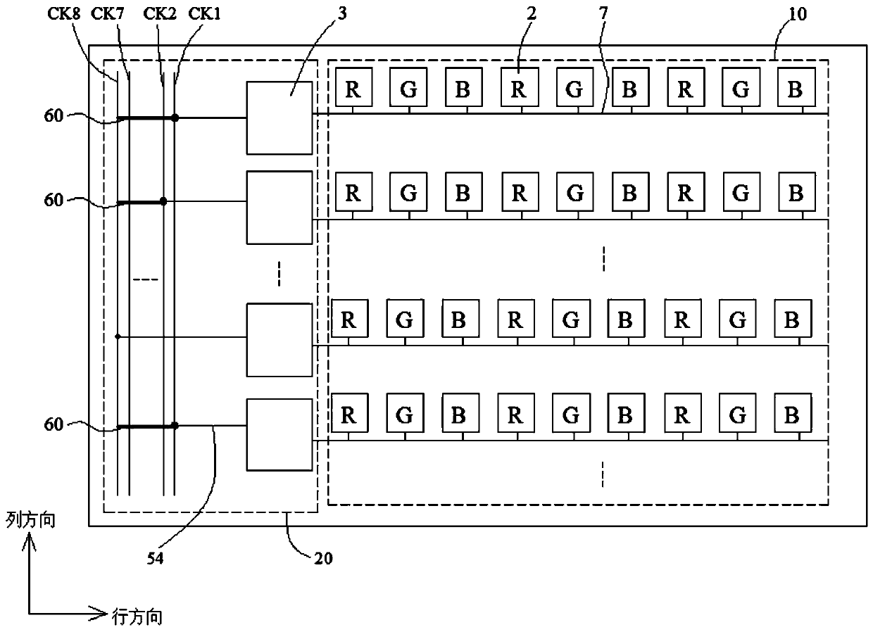
[0071] Such as Figure 5 As shown in , it is a schematic structural diagram of the display panel provided in Embodiment 2 of the present application. The structure of the display panel in this embodiment is the same / similar to the display panel in the first embodiment above, the only difference is that the display panel in this embodiment is a dual-drive display panel, that is, the GOA circuit area 20 is located in the display panel when scanning The two sides of the display area 10 in the line direction. That is, the display panel includes two sets of GOA circuits, and each set of GOA circuits includes cascaded n-level GOA circuit units 3 and N high-frequency clock signal lines, and also includes the compensation unit group 6 . The two GOA circuit areas 20 both include the compensation unit group 6 , and the specific design of the compensation unit group 6 is consistent with the design in the first embodiment above, and will not be repeated here. Wherein, each level of GOA ...
Embodiment 3
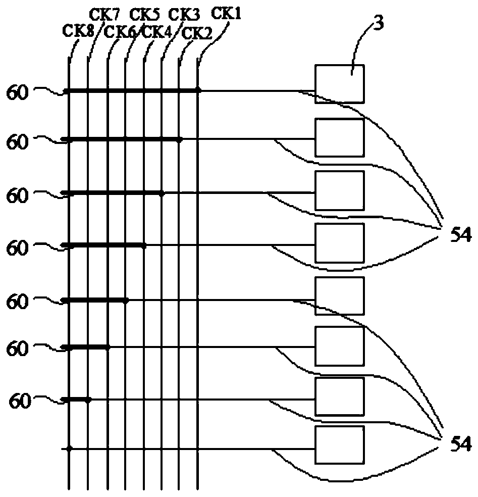
[0074] Such as Figure 6 As shown in FIG. 2 , it is a schematic diagram of a partial structure of a display panel provided in Embodiment 3 of the present application. The structure of the display panel in this embodiment is the same / similar to the display panel in the first embodiment above, the only difference is that the winding method of the compensation unit 60 in this embodiment is a circuitous design, which can further increase the The length of the wiring of the compensation unit 60 and the times of crossing other high-frequency clock signal lines can further increase the compensation capability of the resistance and capacitance of the compensation unit 60 .
[0075] In the display panel of the present application, by setting the compensation unit in the GOA circuit area, the compensation unit can compensate the difference in resistance and capacitance between different clock signals, thereby solving bad display phenomena such as horizontal lines; and by setting the com...
PUM
 Abstract
Description
Claims
Application Information
 - R&D
- Intellectual Property
- Life Sciences
- Materials
- Tech Scout
- Unparalleled Data Quality
- Higher Quality Content
- 60% Fewer Hallucinations
Browse by: Latest US Patents, China's latest patents, Technical Efficacy Thesaurus, Application Domain, Technology Topic, Popular Technical Reports.
© 2025 PatSnap. All rights reserved.Legal|Privacy policy|Modern Slavery Act Transparency Statement|Sitemap|About US| Contact US: help@patsnap.com