Array substrate and manufacturing method thereof, and display panel

An array substrate and substrate technology, applied to electrical components, electrical solid devices, circuits, etc., can solve the problems of reduced pixel aperture ratio, large proportion of non-display area, increased power consumption, etc., to reduce the number and increase the aperture ratio , Reduce the effect of backlight power consumption

Pending Publication Date: 2020-07-24
SHENZHEN CHINA STAR OPTOELECTRONICS SEMICON DISPLAY TECH CO LTD
View PDF7 Cites 3 Cited by
  • Summary
  • Abstract
  • Description
  • Claims
  • Application Information

AI Technical Summary

Problems solved by technology

[0002] With the development of the display panel, the pixel requirements of the display panel are getting higher and higher, the pixel size is getting smaller and smaller, the proportion of the non-display area is getting larger and larger, the aperture area is getting smaller and smaller, and the aperture ratio of the pixel is reduced, which leads to The display panel requires a higher brightness backlight, which will cause the problem of increased power consumption

Method used


Image

  • Array substrate and manufacturing method thereof, and display panel
  • Array substrate and manufacturing method thereof, and display panel
  • Array substrate and manufacturing method thereof, and display panel

Examples


Embodiment Construction

[0027] The application will be described in further detail below in conjunction with the accompanying drawings and embodiments. In particular, the following examples are only used to illustrate the present application, but not to limit the scope of the present application. Likewise, the following embodiments are only some of the embodiments of the present application but not all of them, and all other embodiments obtained by those skilled in the art without creative efforts fall within the protection scope of the present application.

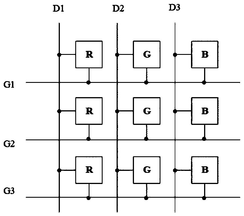
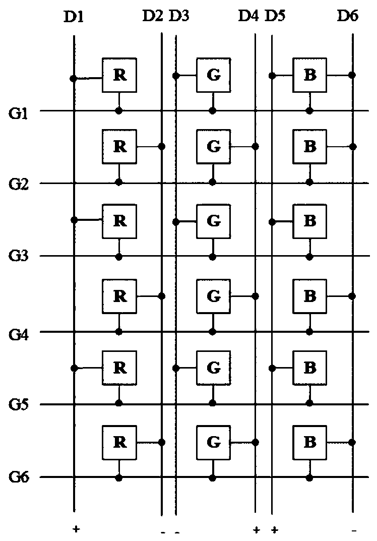
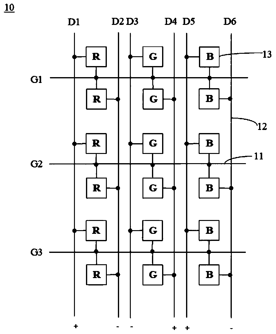
[0028] Such as figure 1 As shown, in a traditional array substrate, each row of pixel units is connected to the same scan line G1 / G2 / G3, and each column of pixel units is connected to the same data line D1 / D2 / D3. High, that is, more and more pixel units, will lead to a shorter and shorter charging time of a single pixel unit. In order to solve this problem, some new pixel unit arrangement structures are proposed in the prior art, for example, ...


PUM


Abstract

The invention relates to a display panel and a manufacturing method thereof, and a display device. The display panel comprises a plurality of scanning lines arranged in a row direction, a plurality ofdata lines arranged in a column direction and a plurality of pixel units which are defined by the scanning lines and the data lines and arranged in rows and columns. Two rows of pixel units are arranged between every two adjacent scanning lines, and each scanning line is electrically connected with the two adjacent rows of pixel units located on the two sides of the scanning line. In this way, one scanning line provides scanning signals for the two adjacent rows of pixel units located on the two sides of the scanning line at the same time, the number of the scanning lines can be reduced, thenan aperture opening ratio of the pixel units in the array substrate can be increased, and backlight power consumption is reduced.

Description

technical field [0001] The present application relates to the field of display technology, in particular to an array substrate, a manufacturing method thereof, and a display panel. Background technique [0002] With the development of the display panel, the pixel requirements of the display panel are getting higher and higher, the pixel size is getting smaller and smaller, the proportion of the non-display area is getting larger and larger, the opening area is getting smaller and smaller, and the aperture ratio of the pixel is reduced, which leads to The display panel requires a higher brightness backlight, which causes a problem of increased power consumption. Contents of the invention [0003] The purpose of the present application is to provide an array substrate, a manufacturing method thereof, and a display panel, so as to increase the pixel aperture ratio and further reduce backlight power consumption. [0004] In order to solve the above problems, an embodiment of ...

Claims


Application Information

Patent Timeline
Patent Type & Authority Applications(China)
IPC IPC(8): H01L27/12
CPCH01L27/124H01L27/1259
Inventor 吕晓文
Owner SHENZHEN CHINA STAR OPTOELECTRONICS SEMICON DISPLAY TECH CO LTD
Why Eureka
Try Eureka