Data enhancement method and system for PCB image defect detection

A PCB board and defect detection technology, which is applied in the field of image recognition, can solve the problems of data enhancement of small-sized missing image samples, inaccurate PCB board image defects, etc., and achieve the effect of enhancing generalization ability, easy detection, and enhancing training data

Active Publication Date: 2020-08-25
CHENGDU UNION BIG DATA TECH CO LTD
View PDF13 Cites 5 Cited by
  • Summary
  • Abstract
  • Description
  • Claims
  • Application Information

AI Technical Summary

Problems solved by technology

[0004] The technical problem to be solved by the present invention is the inaccuracy of the PCB board image defects caused by the lack of filling image samples of small size and inaccurate samples in PCB board image defect detection, and the purpose is to provide a data enhancement method and system for PCB board image defect detection, Solved the problem of data enhancement of small size missing filling image samples in PCB board image defect detection

Method used


Image

  • Data enhancement method and system for PCB image defect detection
  • Data enhancement method and system for PCB image defect detection
  • Data enhancement method and system for PCB image defect detection

Examples


Embodiment 1

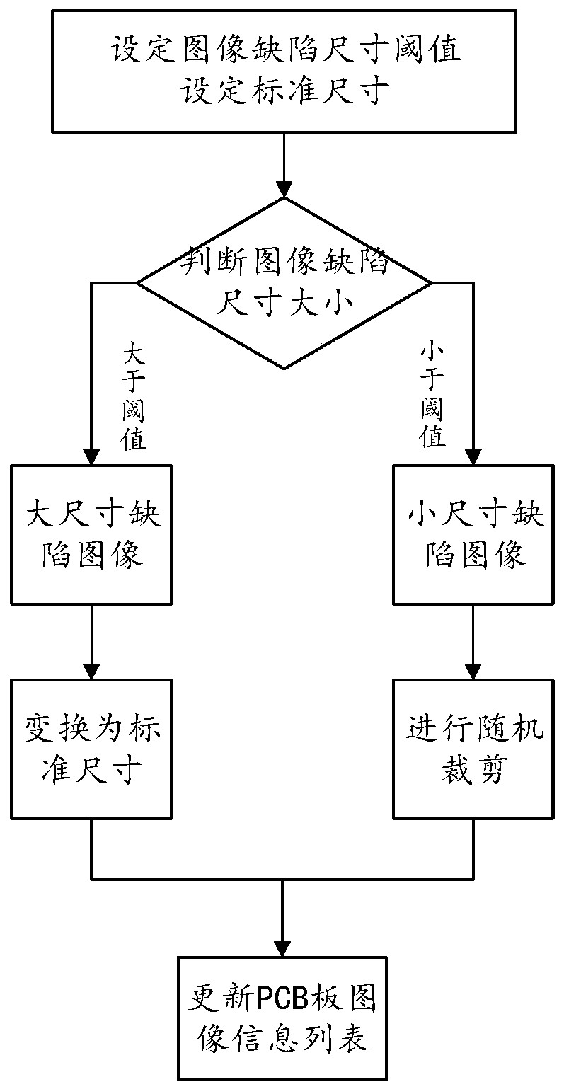
[0045] This embodiment proposes a method for randomly cropping crops for PCB board image defects. This method is applied in the deep learning model training process to enhance data and make it easier to detect small defects in the image. Such as figure 1 shown.

[0046] The steps that this embodiment realizes are as follows:

[0047] Step 1: Set the threshold threshold of the defect size, and judge whether the defect in the image is a large-size defect according to the defect bbox information in the list results of the image information stored on the PCB board. If it is larger than the threshold, it is a large-size defect, otherwise, it is a small-size defect;

[0048] Step 2: If the defect is determined to be a large-size defect in step 1, directly resize the image to crop_size, and update the image matrix, image size, defect bbox and other information in the results list at the same time;

[0049] Step 3: If it is judged in step 1 that the defect is a small-sized defect, c...

Embodiment 2

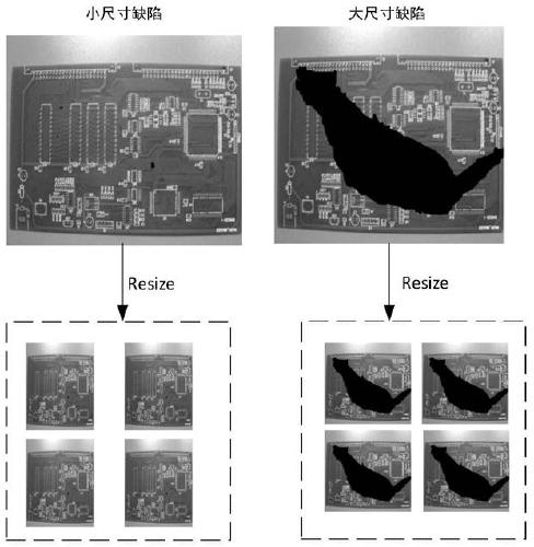
[0064] The applicable scenario of this implementation is defect detection in the PCB panel industry. In order to find the position of the foreign matter in the PCB picture, and classify whether it is a foreign matter or other defect types. The commonly used methods are resize (image scaling) and crop (cropping). The following explains the specific operations of resize and crop and compares the test results:

[0065] 1. The resize method

[0066] Due to the requirements of hardware equipment and computing speed, we generally have to scale the actual picture. Such as figure 2 As shown, no matter what the zoom ratio is, for large-sized defects, zooming has little effect on its detection; for small defects, as the zoom ratio increases, the detection of small defects in the picture becomes more and more difficult, so for the images that exist In the case of small defects, it cannot be resized, and the crop method needs to be adopted.

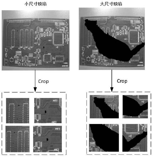
[0067] 2. crop method


PUM


Abstract

The invention discloses a data enhancement method for PCB image defect detection, and the method comprises the steps: setting an image defect size threshold, and setting a standard size; converting the sizes of the image defects of which the image defect sizes are greater than an image defect size threshold value in the PCB image information list into standard sizes, and randomly cutting the imagedefects of which the image defect sizes are smaller than the image defect size threshold value; and updating the PCB image information list. After the PCB image defects are processed for multiple times by adopting the method, the sample number of the small-size defect images is enriched, the training data of the small-size defect images is enhanced, the generalization ability of the PCB image defect detection deep learning model is enhanced, and the small defects of the PCB images are easier to detect.

Description

technical field [0001] The invention relates to the field of image recognition, in particular to a data enhancement method and system for PCB image defect detection. Background technique [0002] When training a deep learning model in image defect detection in the industrial manufacturing panel industry, there are two extreme code size images in the data set. The extremely small code size is a very small black dot, and the extremely large code size is a very large code. It is close to the size of the entire picture. In addition, when distinguishing pictures with small code sizes, it is also necessary to base on whether there is halo, whether the halo is in color, etc. The size of the picture required for training the model under the existing hardware equipment needs to be resized or cropped. The resize method is used to deal with the above extreme situations and to distinguish whether there is a halo or whether it is a color halo. The best way is crop. [0003] The current...

Claims


Application Information

Patent Timeline
Patent Type & Authority Applications(China)
IPC IPC(8): G06T7/00G01N21/956
CPCG06T7/0004G01N21/956G06T2207/10004G06T2207/20132G06T2207/20081G06T2207/30141G01N2021/95638
Inventor 不公告发明人
Owner CHENGDU UNION BIG DATA TECH CO LTD
Why Eureka
Try Eureka