Multiband active metamaterial wave absorber

A metamaterial and wave absorber technology, applied in electrical components, antennas, etc., can solve the problems of non-adjustable wave absorption performance and single frequency, and achieve the effect of simple structure and easy processing and production.

Pending Publication Date: 2020-10-09
陈名松
View PDF0 Cites 3 Cited by
  • Summary
  • Abstract
  • Description
  • Claims
  • Application Information

AI Technical Summary

Problems solved by technology

[0004] What the present invention aims to solve is the problem that the existing metamaterial wave absorber has a single frequency and the wave absorbing performance cannot be adjusted, and provides a multi-band active metamaterial wave absorber

Method used


Image

  • Multiband active metamaterial wave absorber
  • Multiband active metamaterial wave absorber
  • Multiband active metamaterial wave absorber

Examples


Embodiment Construction

[0020] The present invention will be described in detail below in conjunction with the accompanying drawings.

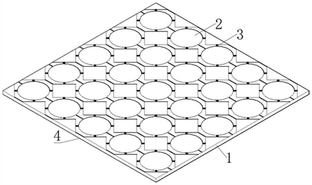
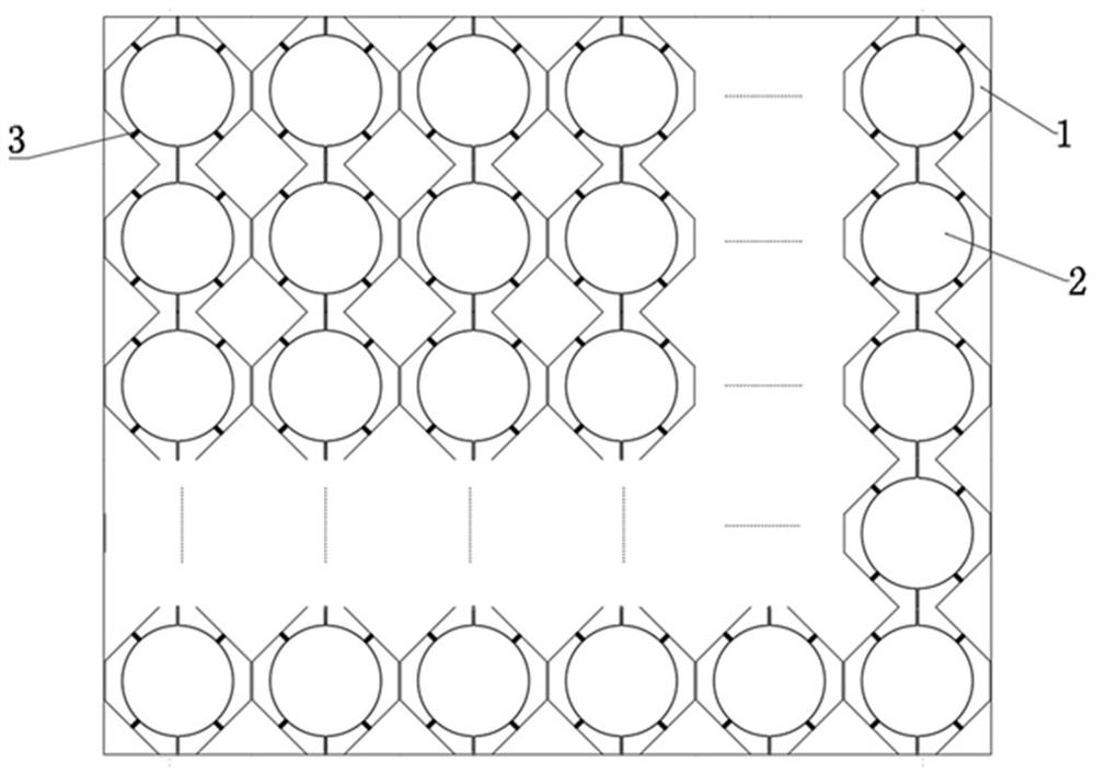
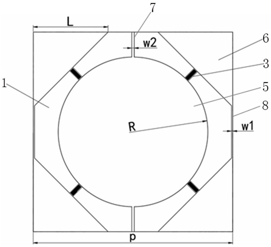
[0021] Such as Figure 1-Figure 3 As shown, a multi-band active metamaterial absorber includes a dielectric substrate 1, a metasurface metal resonant array layer 2 printed on the top surface of the dielectric substrate 1, and a metasurface metal resonant array layer loaded on the metasurface metal resonant array layer 2. The capacitor diode 3 and the metal ground layer printed on the back of the dielectric substrate 1, the metasurface metal resonant array layer 2 is composed of a plurality of unit structures arranged continuously along the X-axis direction and the Y-axis direction of the top surface of the dielectric substrate 1, each Each unit structure comprises a metal disc 5 and four triangular metal patches 6 evenly distributed on the outside of the metal disc 5 outer circumference. In each unit structure, each triangular metal patch 6 and metal disc 5 Varactor...


PUM

PropertyMeasurementUnit
thicknessaaaaaaaaaa
thicknessaaaaaaaaaa
dielectric lossaaaaaaaaaa

Abstract

The invention discloses a multi-band active metamaterial wave absorber. The multi-band active metamaterial wave absorber comprises a dielectric substrate, a metasurface metal resonance array layer printed on the top surface of the dielectric substrate, a varactor diode loaded on the metasurface metal resonance array layer, and a metal grounding layer printed on the back surface of the dielectric substrate. The wave absorber is characterized in that the metasurface metal resonance array layer is composed of a plurality of unit structures which are continuously arranged in the X-axis direction and the Y-axis direction of the top face of the dielectric substrate; each unit structure comprises a metal wafer and four triangular metal patches uniformly distributed on the outer side of the outercircumference of the metal wafer; and in each unit structure, a variable capacitance diode is welded between each triangular metal patch and the metal wafer. The wave absorber has a plurality of waveabsorbing frequency bands, continuous tuning can be carried out by adjusting the bias voltage of the varactor, and the wave absorbing performance of the wave absorber is adjusted.

Description

technical field [0001] The invention relates to the technical field of electromagnetic wave absorption, in particular to a multi-band active metamaterial absorber. Background technique [0002] The absorbing material is a type of functional material that effectively absorbs the electromagnetic waves projected onto its surface and significantly reduces the target echo intensity. Traditional absorbing materials such as ferrite, metal micropowder, silicon carbide, and conductive fibers are thick, heavy, and poor in stability. And other shortcomings, the scope of application is limited. The emergence of new metamaterials overcomes the thickness limitation brought by the diffraction effect to traditional absorbing materials, and has the advantages of thin thickness, light weight, and strong absorption. Metamaterials are artificial materials composed of subwavelength microstructure units arranged according to certain rules. The resonance properties of materials can be tuned by a...

Claims


Application Information

Patent Timeline
Patent Type & Authority Applications(China)
IPC IPC(8): H01Q15/00H01Q17/00
CPCH01Q15/002H01Q15/0026H01Q15/0086H01Q17/007H01Q17/008
Inventor 陈名松梁玉林周奕捷高喜彭麟
Owner 陈名松
Why Eureka
Try Eureka